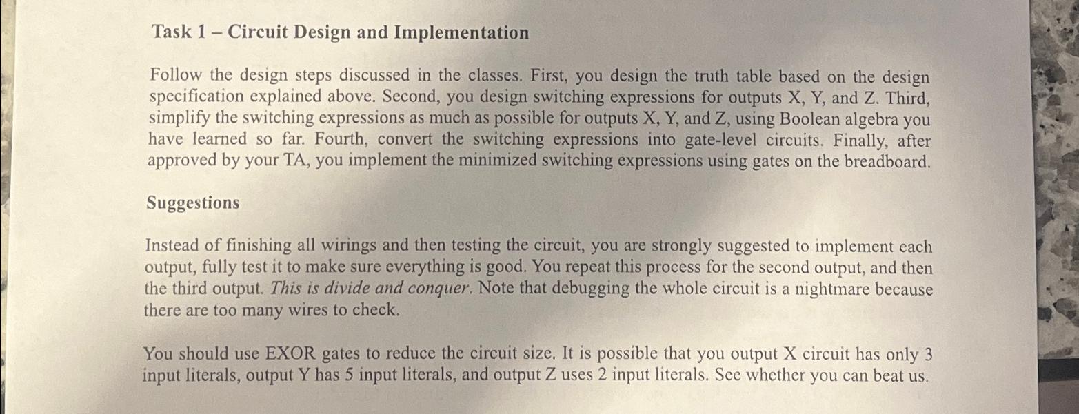
Question: Task 1 - Circuit Design and Implementation Follow the design steps discussed in the classes. First, you design the truth table based on the design
Task Circuit Design and Implementation
Follow the design steps discussed in the classes. First, you design the truth table based on the design specification explained above. Second, you design switching expressions for outputs X Y and Z Third, simplify the switching expressions as much as possible for outputs and using Boolean algebra you have learned so far. Fourth, convert the switching expressions into gatelevel circuits. Finally, after approved by your TA you implement the minimized switching expressions using gates on the breadboard.
Suggestions
Instead of finishing all wirings and then testing the circuit, you are strongly suggested to implement each output, fully test it to make sure everything is good. You repeat this process for the second output, and then the third output. This is divide and conquer. Note that debugging the whole circuit is a nightmare because there are too many wires to check.
You should use EXOR gates to reduce the circuit size. It is possible that you output circuit has only input literals, output has input literals, and output uses input literals. See whether you can beat us

Step by Step Solution
There are 3 Steps involved in it
1 Expert Approved Answer
Step: 1 Unlock


Question Has Been Solved by an Expert!
Get step-by-step solutions from verified subject matter experts
Step: 2 Unlock
Step: 3 Unlock


