Question: N.B: Coding for this task must be done by using the software 'Vivado' The 7 Segment Display Driver Introduction The aim of this task 2

N.B: Coding for this task must be done by using the software 'Vivado'

N.B: Coding for this task must be done by using the software'Vivado' The 7 Segment Display Driver Introduction The aim of this task2 is to design and test a 4 Digit 7-segment Display driver

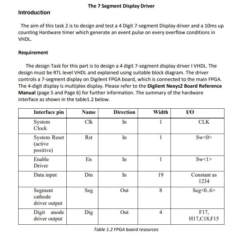
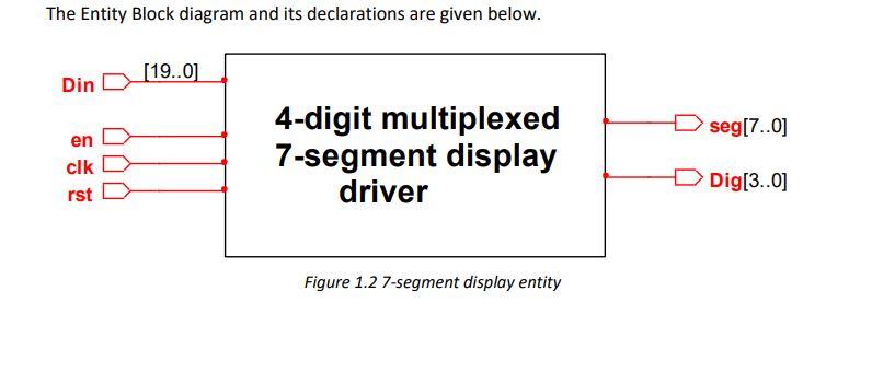
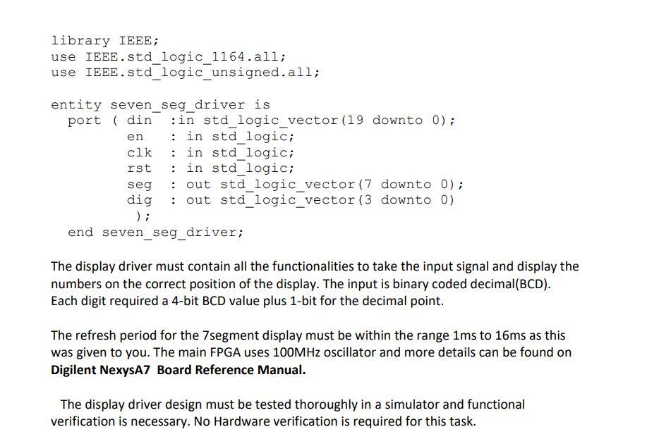
The 7 Segment Display Driver Introduction The aim of this task 2 is to design and test a 4 Digit 7-segment Display driver and a 10ms up counting Hardware timer which generate an event pulse on every overflow conditions in VHDL. Requirement The design Task for this part is to design a 4 digit 7-segment display driver I VHDL. The design must be RTL level VHDL and explained using suitable block diagram. The driver controls a 7-segment display on Digilent FPGA board, which is connected to the main FPGA. The 4-digit display is multiplex display. Please refer to the Digilent Nexys2 Board Reference Manual (page 5 and Page 6) for further information. The summary of the hardware interface as shown in the table1.2 below. Name Direction Width I/O Clk In 1 CLK Rst In Sw Interface pin System Clock System Reset (active positive) Enable Driver Data input En In 1 Sw Din In 19 Constant as 1234 Seg Out 8 Seg Segment cathode driver output Digit anode driver output Dig Out 4 F17, H17,C18,F15 Table 1.2 FPGA board resources The Entity Block diagram and its declarations are given below. [19..0] Din seg[7..0] en 4-digit multiplexed 7-segment display driver clk rst Dig[3..0] Figure 1.2 7-segment display entity library IEEE; use IEEE.std_logic_1164.all; use IEEE.std_logic_unsigned.all; entity seven_seg_driver is port ( din :in std_logic_vector (19 downto 0); en : in std_logic; clk : in std_logic; rst : in std logic; seg : out std_logic_vector (7 downto 0); dig : out std_logic_vector (3 downto 0) ); end seven_seg_driver; The display driver must contain all the functionalities to take the input signal and display the numbers on the correct position of the display. The input is binary coded decimal(BCD). Each digit required a 4-bit BCD value plus 1-bit for the decimal point. The refresh period for the 7 segment display must be within the range 1ms to 16ms as this was given to you. The main FPGA uses 100MHz oscillator and more details can be found on Digilent NexysA7 Board Reference Manual. The display driver design must be tested thoroughly in a simulator and functional verification is necessary. No Hardware verification is required for this task

Step by Step Solution

There are 3 Steps involved in it

1 Expert Approved Answer
Step: 1 Unlock blur-text-image
Question Has Been Solved by an Expert!

Get step-by-step solutions from verified subject matter experts

Step: 2 Unlock
Step: 3 Unlock

Students Have Also Explored These Related Databases Questions!