

Question: Test Plan Development for an IP block - thought process Functional Architecture, Circuit components, DFT architecture Digital, analog or mixed? What type of DFT hooks
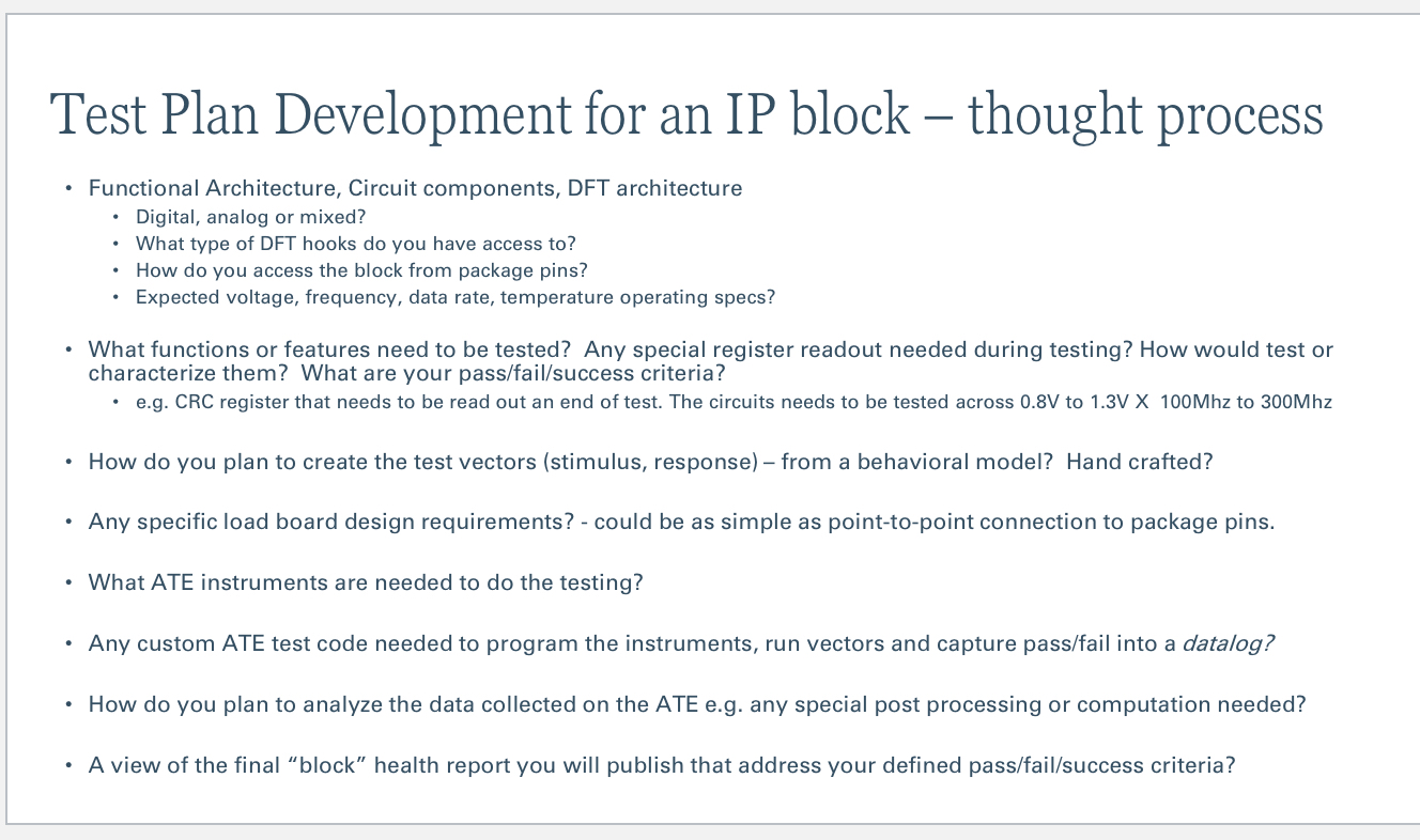
Test Plan Development for an IP block thought process
Functional Architecture, Circuit components, DFT architecture
Digital, analog or mixed?
What type of DFT hooks do you have access to
How do you access the block from package pins?
Expected voltage, frequency, data rate, temperature operating specs?
What functions or features need to be tested? Any special register readout needed during testing? How would test or
characterize them? What are your passfailsuccess criteria?
eg CRC register that needs to be read out an end of test. The circuits needs to be tested across V to V X Mhz to Mhz
How do you plan to create the test vectors stimulus response from a behavioral model? Hand crafted?
Any specific load board design requirements? could be as simple as pointtopoint connection to package pins.
What ATE instruments are needed to do the testing?
Any custom ATE test code needed to program the instruments, run vectors and capture passfail into a datalog?
How do you plan to analyze the data collected on the ATE eg any special post processing or computation needed?
A view of the final "block" health report you will publish that address your defined passfailsuccess criteria?
Answer the Questions on Ditigal Clock PLEASE
Step by Step Solution
There are 3 Steps involved in it
1 Expert Approved Answer
Step: 1 Unlock

To develop a test plan for an IP block specifically focusing on a digital clock consider the following aspects outlined in the provided material Step ... View full answer
Question Has Been Solved by an Expert!
Get step-by-step solutions from verified subject matter experts
Step: 2 Unlock
Step: 3 Unlock