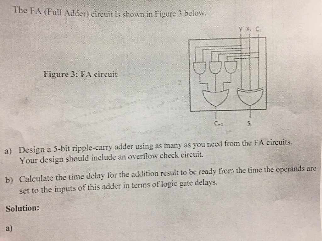
Question: The FA (Full Adder) circuit is shown in Figure 3 below Figure 3: FA circuit S. a) Design a 5-bit ripple-carry adder using as many

The FA (Full Adder) circuit is shown in Figure 3 below Figure 3: FA circuit S. a) Design a 5-bit ripple-carry adder using as many as you need from the FA circuits. Your design should include an overflow check circuit. Calculate the time delay for the addition result to be ready from the time the operands are set to the inputs of this adder in terms of logic gate delays. b) Solution: a)
Step by Step Solution
There are 3 Steps involved in it

Get step-by-step solutions from verified subject matter experts


