

Question: the flip flop excitation equations for binary state assignment ( two state variables ) , show the schematic CSbarCLK Init CLK St Figure 3. The
the flip flop excitation equations for binary state assignment ( two state variables ) , show the schematic
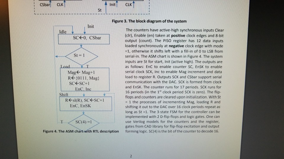
CSbarCLK Init CLK St Figure 3. The block diagram of the system Init The counters have active-high synchronous inputs Clear (clr), Enable (en) taken at positive clock edges and 8-bit output (count). The PISO register has 12 data inputs loaded synchronously at negative clock edge with mode -1, otherwise it shifts left with a fill-in of 0 to LSB from serial-in. The ASM chart is shown in Figure 4. The system inputs are St for start, Init (active high). The outputs are as follows: EnC to enable counter SC, EnSK to enable serial clock SCK, Inc to enable Mag increment and data load to register R. Outputs SCK and CSbar support serial communication with the DAC. SCK is formed from clock and EnSK. The counter runs for 17 periods. SCK runs for 16 periods (in the 1st clock period SCK is zero). The flip- SCE0, CSbar St-1 Load Mag? Mag+1 R? 101 1 1, Mag: SCE SC+1 nc Sh flops and counters are cleared upon initialization. With St REsl(R), SC SC+1 1 the processes of incrementing Mag, loading R and shifting it out to the DAC over 16 clock periods repeat as long as St -1. The 3-state FSM for the controller can be implemented with 2 D-flip-flops and logic gates. One can use Verilog models for the counters and the register, gates from CAD library for flip-flop excitation and output EnC, EnSK TSC(4)-1 Figure 4. The ASM chart-with RTL description forming logic. SC(4) is the bit of the counter to decode 16. CSbarCLK Init CLK St Figure 3. The block diagram of the system Init The counters have active-high synchronous inputs Clear (clr), Enable (en) taken at positive clock edges and 8-bit output (count). The PISO register has 12 data inputs loaded synchronously at negative clock edge with mode -1, otherwise it shifts left with a fill-in of 0 to LSB from serial-in. The ASM chart is shown in Figure 4. The system inputs are St for start, Init (active high). The outputs are as follows: EnC to enable counter SC, EnSK to enable serial clock SCK, Inc to enable Mag increment and data load to register R. Outputs SCK and CSbar support serial communication with the DAC. SCK is formed from clock and EnSK. The counter runs for 17 periods. SCK runs for 16 periods (in the 1st clock period SCK is zero). The flip- SCE0, CSbar St-1 Load Mag? Mag+1 R? 101 1 1, Mag: SCE SC+1 nc Sh flops and counters are cleared upon initialization. With St REsl(R), SC SC+1 1 the processes of incrementing Mag, loading R and shifting it out to the DAC over 16 clock periods repeat as long as St -1. The 3-state FSM for the controller can be implemented with 2 D-flip-flops and logic gates. One can use Verilog models for the counters and the register, gates from CAD library for flip-flop excitation and output EnC, EnSK TSC(4)-1 Figure 4. The ASM chart-with RTL description forming logic. SC(4) is the bit of the counter to decode 16
Step by Step Solution
There are 3 Steps involved in it

Get step-by-step solutions from verified subject matter experts