

Question: The timing diagram below is for the 8-bit register block shown. Complete the timing diagram by filling in the output (q) signal. 3. U1 load
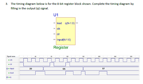
The timing diagram below is for the 8-bit register block shown. Complete the timing diagram by filling in the output (q) signal. 3. U1 load q(N-1:0) clk cir Input(N-1:0) Register Signal name dr input 2D 6A 57 load +
Step by Step Solution
There are 3 Steps involved in it
1 Expert Approved Answer
Step: 1 Unlock

Question Has Been Solved by an Expert!
Get step-by-step solutions from verified subject matter experts
Step: 2 Unlock
Step: 3 Unlock