

Question: This is digital logic lab(using quartiz 13.3) I couldnt solve it , I need help, especially operation 1&2 ?? , notice that were not allowed
 This is digital logic lab(using quartiz 13.3) I couldnt solve it , I need help, especially operation 1&2 ?? , notice that were not allowed to use truth table to solve it we have to write verilog code
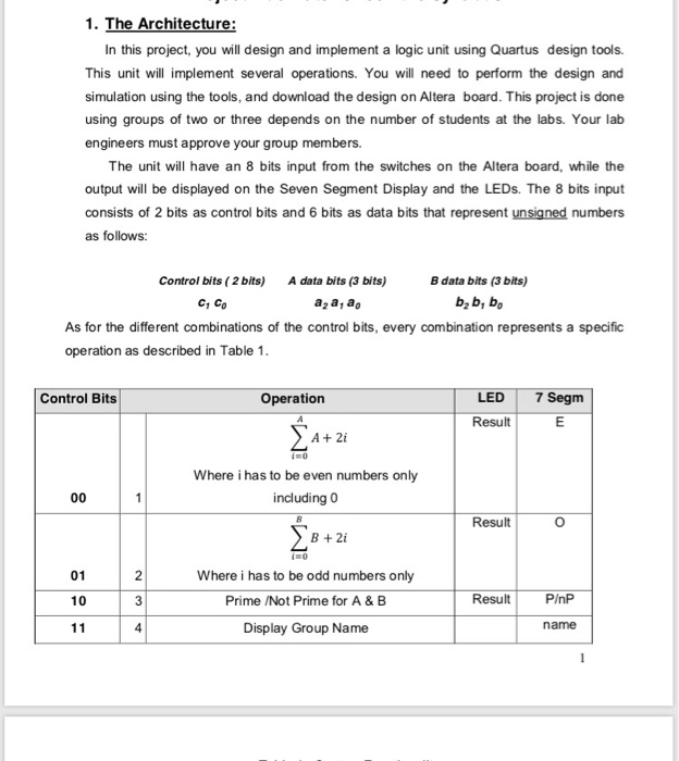
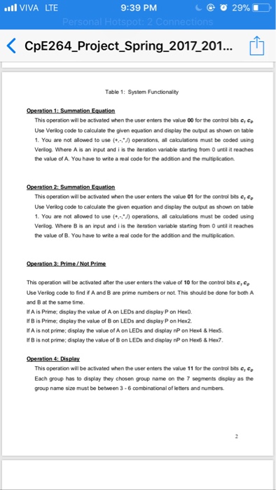
 1. The Architecture: In this project, you will design and implement a logic unit using Quartus design tools. This unit will implement several operations. You will need to perform the design and simulation using the tools, and download the design on Altera board. This project is done using groups of two or three depends on the number of students at the labs. Your lab engineers must approve your group members. The unit will have an 8 bits input from the switches on the Altera board, while the output will be displayed on the Seven Segment Display and the LEDs. The 8 bits input consists of 2 bits as control bits and 6 bits as data bits that represent unsigned numbers as follows: Control bits ( 2 bits) A data bits (3 bits) B data bits (3 bits) C1 Co a2 a1 ao b2 b, bo As for the different combinations of the control bits, every combination represents a specific operation as described in Table 1 LED 7 Segm Result Control Bits Operation A 2i Where i has to be even numbers only including Result B +2i 01 Where i has to be odd numbers only Prime /Not Prime for A & B Display Group Name 10 ResultPP name
Step by Step Solution
There are 3 Steps involved in it

Get step-by-step solutions from verified subject matter experts