

Question: TRONG BNG OMMUNITY COLLEGE Question 1 (total 18 marks) A chip has the following pinout diagram that also shows the pin names and internal
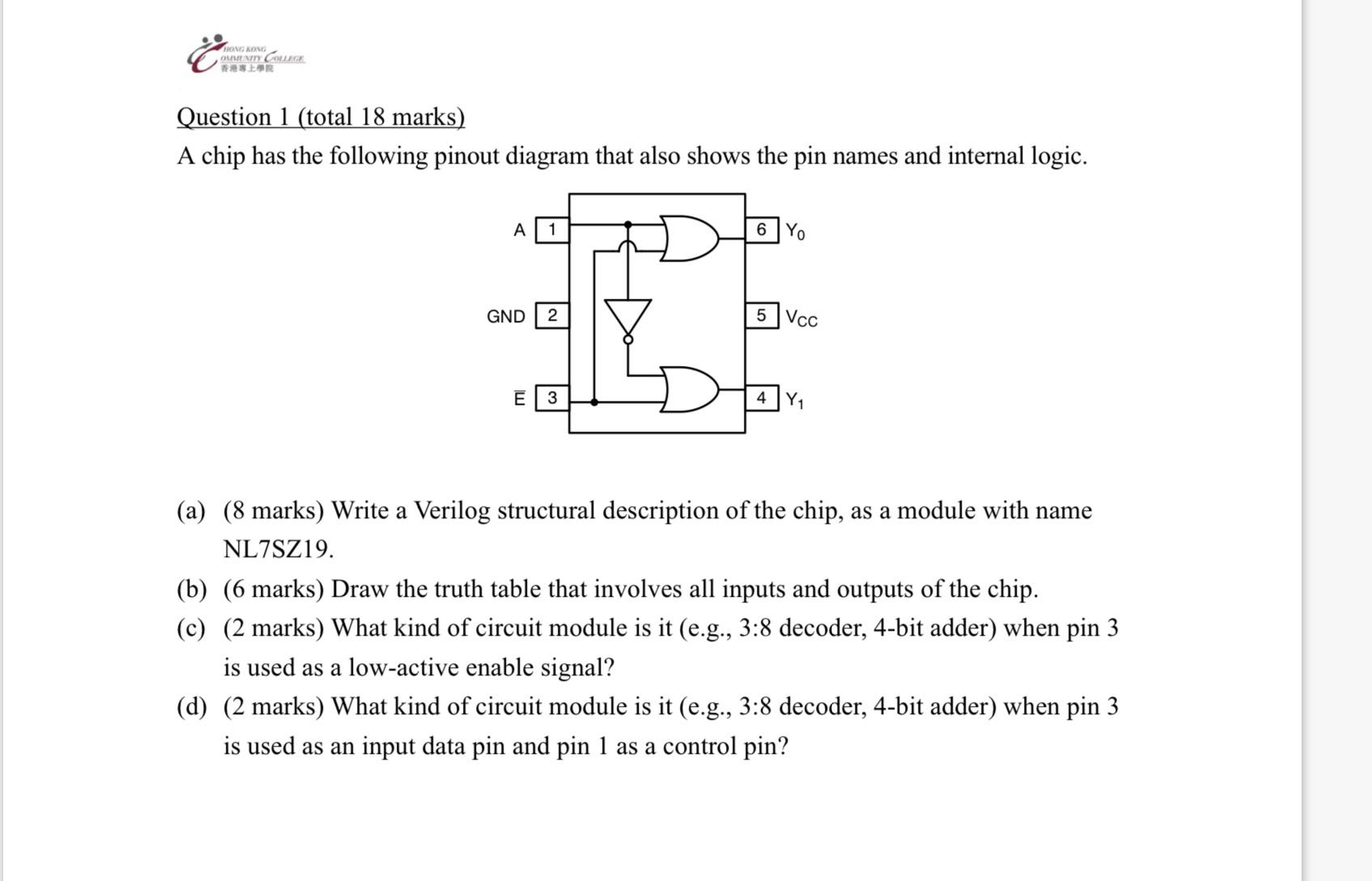
TRONG BNG OMMUNITY COLLEGE Question 1 (total 18 marks) A chip has the following pinout diagram that also shows the pin names and internal logic. A GND 1 2 E 3 6 Yo 5 Vcc 4 Y (a) (8 marks) Write a Verilog structural description of the chip, as a module with name NL7SZ19. (b) (6 marks) Draw the truth table that involves all inputs and outputs of the chip. (c) (2 marks) What kind of circuit module is it (e.g., 3:8 decoder, 4-bit adder) when pin 3 is used as a low-active enable signal? (d) (2 marks) What kind of circuit module is it (e.g., 3:8 decoder, 4-bit adder) when pin 3 is used as an input data pin and pin 1 as a control pin?
Step by Step Solution
There are 3 Steps involved in it

Get step-by-step solutions from verified subject matter experts