

Question: Using Quartus Prime, show code and procedure with explanation pls! Will uplike for good answer with decent explanation - Learn to design a simple arithmetic
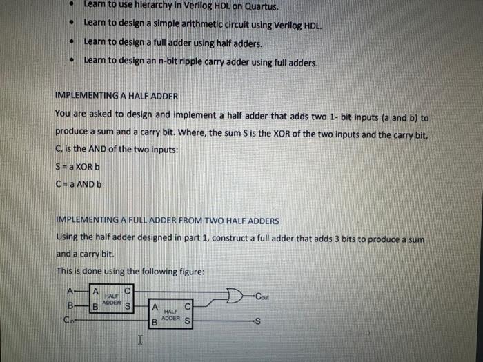
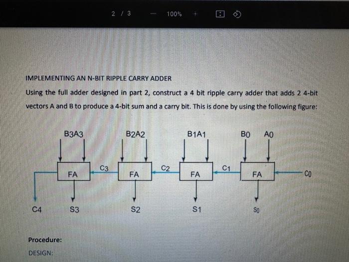
- Learn to design a simple arithmetic circuit using Verilog HDL. - Learn to design a full adder using half adders. - Learn to design an n-bit ripple carry adder using full adders. IMPLEMENTING A HALF ADDER You are asked to design and implement a half adder that adds two 1- bit inputs (a and b ) to produce a sum and a carry bit. Where, the sum S is the XOR of the two inputs and the carry bit, C, is the AND of the two inputs: S=aORbc=aANDb IMPLEMENTING A FULL ADDER FROM TWO HALF ADDERS Using the half adder designed in part 1 , construct a full adder that adds 3 bits to produce a sum and a carry bit. This is done using the following figure: IMPLEMENTING AN N-BIT RIPPLE CARRY ADDER Using the full adder designed in part 2, construct a 4 bit ripple carry adder that adds 2 4-bit vectors A and B to produce a 4-bit sum and a carry bit. This is done by using the following figure: Procedure: DESIGNE 1) Open Quartus Prime 15.1 Web Edition. 2) Create a new project (name it RCadder) ) using the New Project Wizard and place it in the folder My Documents Quartus. Select Custom Design and In Family \& Device Settings Select: Cyclone IV E - EP4CE115F29C7 3) Create a new Verilog HDL design file and Save it in the same folder of the project. 4) Create a module and call it HA. In it write the Verilog code for a half adder, as described above. 5) Create a second module and call it FA. Use instances of the HA module, and the appropriate wires to write the Verilog code of a full adder, as described above. 6) Create the main module, having the same name as the project name (RC_adder) having two 4-bit inputs (a and b), a carry in bit input, a carry out output, and a 4-bit Sum output. Use instances of the FA module, and the appropriate wires to write the Verilog code of a 4-bit ripple carry adder as described above. 7) Check the code for syntax errors using the Analyze tool. 8) Compile the cesign and check for logical or design errors
Step by Step Solution
There are 3 Steps involved in it

Get step-by-step solutions from verified subject matter experts