

Question: When clock and data are from SoC to SPI, what is the setup time ( in ps ) seen at SPI device interface ports (
When clock and data are from SoC to SPI, what is the setup timein ps seen at SPI device interface ports marked with an arrow.
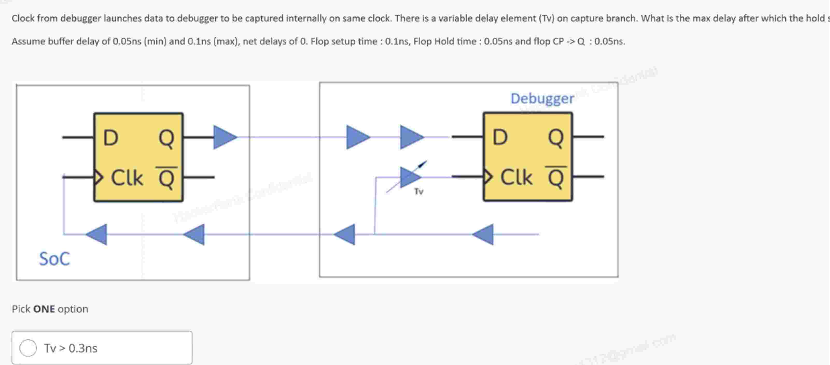
Clock from debugger launches data to debugger to be captured internally on same clock. There is a variable delay element Tv on capture branch. What is the max delay after which the hold is seen
Assume buffer delay of nsmin and ns max net delays of Flop setup time : ns Flop Hold time ; ns and flop CP rarrQ:ns
Pick ONE option
a tvns btvns ctvns dtvns
Step by Step Solution
There are 3 Steps involved in it
1 Expert Approved Answer
Step: 1 Unlock

Question Has Been Solved by an Expert!
Get step-by-step solutions from verified subject matter experts
Step: 2 Unlock
Step: 3 Unlock