

Question: - y2 2. In this problem, we are interested to build an audio amplifier with a gain of 10. Assume the speaker to drive with
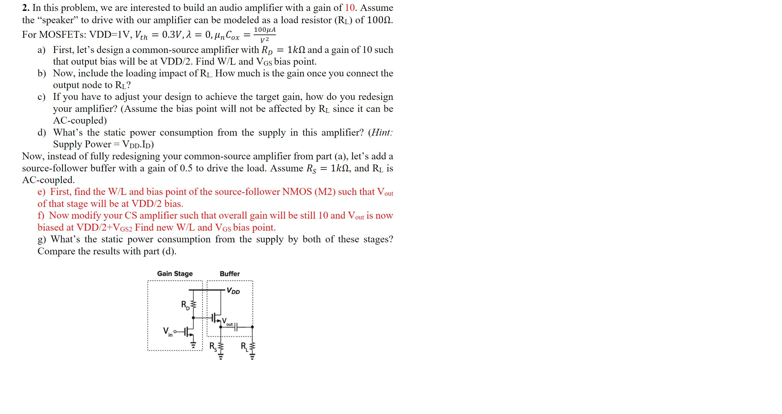
- y2 2. In this problem, we are interested to build an audio amplifier with a gain of 10. Assume the speaker to drive with our amplifier can be modeled as a load resistor (RL) of 10012. 100uA For MOSFETs: VDD=1V, Vth 0.3V, 2 = 0, Un Cox a) First, let's design a common-source amplifier with RD 1ks and a gain of 10 such that output bias will be at VDD/2. Find W/L and Vgs bias point. b) Now, include the loading impact of Rl. How much is the gain once you connect the output node to R? c) If you have to adjust your design to achieve the target gain, how do you redesign your amplifier? (Assume the bias point will not be affected by Ri since it can be AC-coupled) d) What's the static power consumption from the supply in this amplifier? (Hint: Supply Power = VDD.ID) Now, instead of fully redesigning your common-source amplifier from part (a), let's add a source-follower buffer with a gain of 0.5 to drive the load. Assume Rs 1k12, and Ri is AC-coupled. e) First, find the W/L and bias point of the source-follower NMOS (M2) such that Vout of that stage will be at VDD/2 bias. f) Now modify your CS amplifier such that overall gain will be still 10 and Vout is now biased at VDD/2+VGs2 Find new W/L and Vos bias point. g) What's the static power consumption from the supply by both of these stages? Compare the results with part (d). = Gain Stage Buffer VOD R. out VE in no W11 RE - y2 2. In this problem, we are interested to build an audio amplifier with a gain of 10. Assume the speaker to drive with our amplifier can be modeled as a load resistor (RL) of 10012. 100uA For MOSFETs: VDD=1V, Vth 0.3V, 2 = 0, Un Cox a) First, let's design a common-source amplifier with RD 1ks and a gain of 10 such that output bias will be at VDD/2. Find W/L and Vgs bias point. b) Now, include the loading impact of Rl. How much is the gain once you connect the output node to R? c) If you have to adjust your design to achieve the target gain, how do you redesign your amplifier? (Assume the bias point will not be affected by Ri since it can be AC-coupled) d) What's the static power consumption from the supply in this amplifier? (Hint: Supply Power = VDD.ID) Now, instead of fully redesigning your common-source amplifier from part (a), let's add a source-follower buffer with a gain of 0.5 to drive the load. Assume Rs 1k12, and Ri is AC-coupled. e) First, find the W/L and bias point of the source-follower NMOS (M2) such that Vout of that stage will be at VDD/2 bias. f) Now modify your CS amplifier such that overall gain will be still 10 and Vout is now biased at VDD/2+VGs2 Find new W/L and Vos bias point. g) What's the static power consumption from the supply by both of these stages? Compare the results with part (d). = Gain Stage Buffer VOD R. out VE in no W11 RE
Step by Step Solution
There are 3 Steps involved in it

Get step-by-step solutions from verified subject matter experts