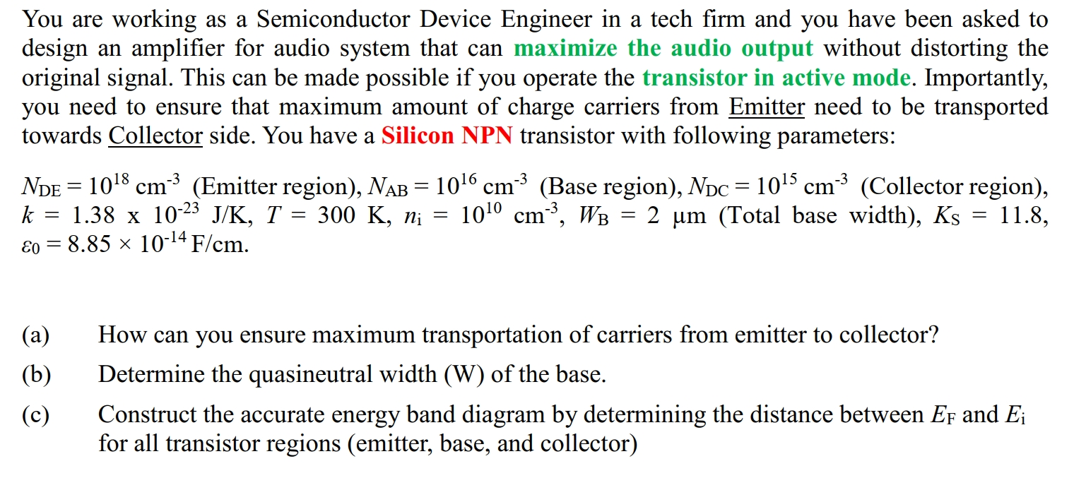
Question: You are working as a Semiconductor Device Engineer in a tech firm and you have been asked to design an amplifier for audio system that

You are working as a Semiconductor Device Engineer in a tech firm and you have been asked to design an amplifier for audio system that can maximize the audio output without distorting the original signal. This can be made possible if you operate the transistor in active mode. Importantly, you need to ensure that maximum amount of charge carriers from Emitter need to be transported towards Collector side. You have a Silicon NPN transistor with following parameters: NDE = 1018 cm- (Emitter region), NAB = 1016 cm- (Base region), Npc = 1015 cm" (Collector region), k = 1.38 x 10⁻²³ J/K, T 300 K, ni = 1010 cm", WB = 2 um (Total base width), Ks 11.8, 0 = 8.85 x 10⁻¹⁴ F/cm. = = (a) (b) How can you ensure maximum transportation of carriers from emitter to collector? Determine the quasineutral width (W) of the base. Construct the accurate energy band diagram by determining the distance between EF and E; for all transistor regions (emitter, base, and collector) (c) You are working as a Semiconductor Device Engineer in a tech firm and you have been asked to design an amplifier for audio system that can maximize the audio output without distorting the original signal. This can be made possible if you operate the transistor in active mode. Importantly, you need to ensure that maximum amount of charge carriers from Emitter need to be transported towards Collector side. You have a Silicon NPN transistor with following parameters: NDE = 1018 cm- (Emitter region), NAB = 1016 cm- (Base region), Npc = 1015 cm" (Collector region), k = 1.38 x 10⁻²³ J/K, T 300 K, ni = 1010 cm", WB = 2 um (Total base width), Ks 11.8, 0 = 8.85 x 10⁻¹⁴ F/cm. = = (a) (b) How can you ensure maximum transportation of carriers from emitter to collector? Determine the quasineutral width (W) of the base. Construct the accurate energy band diagram by determining the distance between EF and E; for all transistor regions (emitter, base, and collector) (c)
Step by Step Solution
There are 3 Steps involved in it

Get step-by-step solutions from verified subject matter experts


