

(a) Redesign the class-AB output stage in Figure 8.34 using enhancementmode MOSFETs. Let (R_{3}=R_{4}=0). Sketch the circuit....
Question:
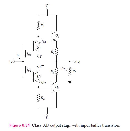
(a) Redesign the class-AB output stage in Figure 8.34 using enhancementmode MOSFETs. Let \(R_{3}=R_{4}=0\). Sketch the circuit.
(b) Assume bias voltages of \(V^{+}=10 \mathrm{~V}\) and \(V^{-}=-10 \mathrm{~V}\). Assume the threshold voltages of the \(\mathrm{n}\)-channel devices are \(V_{T N}=1 \mathrm{~V}\) and the threshold voltages of the p-channel devices are \(V_{T P}=-1 \mathrm{~V}\). Also assume the conduction parameters are \(K_{p 1}=K_{n 2}=2 \mathrm{~mA} / \mathrm{V}^{2}\) and \(K_{n 3}=K_{p 4}=5 \mathrm{~mA} / \mathrm{V}^{2}\). Determine \(R_{1}\) and \(R_{2}\) such that the quiescent drain currents in the output transistors are \(5 \mathrm{~mA}\) (for \(v_{I}=v_{O}=0\) ).
(c) Using the results of part (b), find the currents in \(M_{1}\) and \(M_{2}\).
(d) If \(R_{L}=150 \Omega\), determine the current in each transistor, the input voltage \(v_{I}\), and the power delivered to the load if \(v_{O}=3.5 \mathrm{~V}\).
Step by Step Answer:

This question has not been answered yet.
You can Ask your question!


Microelectronics Circuit Analysis And Design
ISBN: 9780071289474
4th Edition
Authors: Donald A. Neamen
