

Design a voltage regulator circuit such as shown in Figure P2.21 so that (V_{L}=7.5 mathrm{~V}). The Zener
Question:
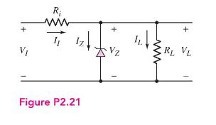
Design a voltage regulator circuit such as shown in Figure P2.21 so that \(V_{L}=7.5 \mathrm{~V}\). The Zener diode voltage is \(V_{Z}=7.5 \mathrm{~V}\) at \(I_{Z}=10 \mathrm{~mA}\). The incremental diode resistance is \(r_{z}=12 \Omega\). The nominal supply voltage is \(V_{I}=12 \mathrm{~V}\) and the nominal load resistance is \(R_{L}=1 \mathrm{k} \Omega\).
(a) Determine \(R_{i}\).
(b) If \(V_{I}\) varies by \(\pm 10\) percent, calculate the source regulation. What is the variation in output voltage?
(c) If \(R_{L}\) varies over the range of \(1 \mathrm{k} \Omega \leq R_{L} \leq \infty\), what is the variation in output voltage? Determine the load regulation.
Figure P2.21:-
Step by Step Answer:
a Ri200 ...View the full answer


Microelectronics Circuit Analysis And Design
ISBN: 9780071289474
4th Edition
Authors: Donald A. Neamen
