

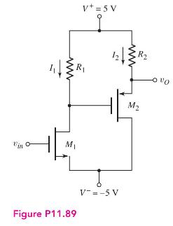
The bias currents in the circuit shown in Figure P11.89 are (I_{1}=0.25 mathrm{~mA}) and (I_{2}=1.0 mathrm{~mA}). The
Question:
The bias currents in the circuit shown in Figure P11.89 are \(I_{1}=0.25 \mathrm{~mA}\) and \(I_{2}=1.0 \mathrm{~mA}\). The transistor parameters are \(K_{n}=0.5 \mathrm{~mA} / \mathrm{V}^{2}\), \(K_{p}=1.0 \mathrm{~mA} / \mathrm{V}^{2}, V_{T N}=0.8 \mathrm{~V}, V_{T P}=-0.8 \mathrm{~V}\), and \(\lambda_{n}=\lambda_{p}=0.02 \mathrm{~V}^{-1}\).
(a) Determine the resistor values \(R_{1}\) and \(R_{2}\) such that the dc value of the output voltage is zero.
(b) Sketch the small-signal equivalent circuit and find the small-signal transistor parameters.
(c) Determine the small-signal voltage gain \(A_{v}=v_{o} / v_{i n}\).
(d) Determine the output resistance \(R_{o}\).
Fantastic news! We've Found the answer you've been seeking!
Step by Step Answer:

Answered By
Emel Khan
I have the ability to effectively communicate and demonstrate concepts to students. Through my practical application of the subject required, I am able to provide real-world examples and clarify complex ideas. This helps students to better understand and retain the information, leading to improved performance and confidence in their abilities. Additionally, my hands-on approach allows for interactive lessons and personalized instruction, catering to the individual needs and learning styles of each student.
2+ Reviews
10+ Question Solved
Related Book For 

Microelectronics Circuit Analysis And Design
ISBN: 9780071289474
4th Edition
Authors: Donald A. Neamen
Question Posted:
