

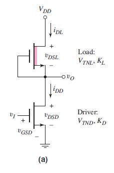
The NMOS inverter with depletion load is shown in Figure 16.7(a). The bias is (V_{D D}=2.5 mathrm{~V}).
Question:
The NMOS inverter with depletion load is shown in Figure 16.7(a). The bias is \(V_{D D}=2.5 \mathrm{~V}\). The transistor parameters are \(V_{T N D}=0.5 \mathrm{~V}\) and \(V_{T N L}=-1 \mathrm{~V}\). The width-to-length ratio of the load device is \(W / L=1\).
(a) Design the driver transistor such that \(v_{O}=0.05 \mathrm{~V}\) when the input is a logic 1.
(b) What is the power dissipated in the circuit when \(v_{I}=2.5 \mathrm{~V} ?\)
Figure 16.7(a):-
Fantastic news! We've Found the answer you've been seeking!
Step by Step Answer:

Answered By
Elias Gichuru
am devoted to my work and dedicated in helping my clients accomplish their goals and objectives,providing the best for all tasks assigned to me as a freelancer,providing high quality work that yields high scores.promise to serve them earnestly and help them achieve their goals.i have the needed expertise,knowledge and experience to handle their tasks.
325+ Reviews
859+ Question Solved
Related Book For 

Microelectronics Circuit Analysis And Design
ISBN: 9780071289474
4th Edition
Authors: Donald A. Neamen
Question Posted:
