

Question: Thermal stress testing is a common procedure used to assess the reliability of an electronic package. Typically, thermal stresses are induced in soldered or wired
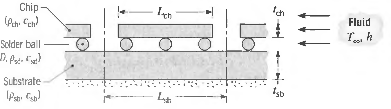
Thermal stress testing is a common procedure used to assess the reliability of an electronic package. Typically, thermal stresses are induced in soldered or wired connections to reveal mechanisms that could cause failure and must therefore be corrected before the product is released. As an example of the procedure, consider an array of silicon chips (Pch = 2300 kg/m3, Cch = 710J/kg ∙ K) joined to an alumina substrate (Psb = 4000 kg/m3 ∙ csb = 770 J/kg ∙ K) by solder balls (Psd = 11,000 kg/m3, Csd = 130 J/kg ∙ K). Each chip of width Lch and thickness tch is joined to a unit substrate section of width Lsb and thickness tch by solder balls of diameter D.
A thermal stress test begins by subjecting the multichip module, which is initially at room temperature, to a hot fluid stream and subsequently cooling the module by exposing it to a cold fluid stream. The process is repeated for a prescribed number of cycles to assess the integrity of the soldered connections.
(a) As a first approximation, assume that there is negligible heat transfer between the components (chip/solder/substrate) of the module and that the thermal response of each component may be determined from a lumped capacitance analysis involving the same convection coefficient h. Assuming no reduction in surface area due to contact between a solder ball and the chip or substrate, obtain expressions for the thermal time constant of each component. Heat transfer is to all surfaces of a chip, but to only the top surface of the substrate. Evaluate the three time constants for Lch = 15 mm, tch = 2 mm. Lsb = 25 mm, tsb = 10 mm, D = 2 mm, and a value of h = 50 W/m2 ∙ K, which is characteristic of an air stream. Compute and plot the temperature histories of the three components for the heating portion of a cycle, with Ti = 20°C and T∞ = 80°C. At what time does each component experience 99% of its maximum possible temperature rise, that is, (T – Ti) / (T∞ - Ti) = 0.99? If the maximum stress on a solder ball corresponds to the maximum difference between its temperature and that of the chip or substrate, when will this maximum occur?
(b) To reduce the time required to complete a stress test, a dielectric liquid could be used in lieu of air to provide a larger convection coefficient of h = 200 W/m2 ∙ K. What is the corresponding savings in time for each component to achieve 99% of its maximum possible temperature rise?
Chip- (Peno Cchd "ch Lch Fluid Te, h Solder ball D. Psd. Csa) Substrate (Psbo Csb) Lsb
Step by Step Solution
3.46 Rating (159 Votes )
There are 3 Steps involved in it
KNOWN Dimensions initial temperature and thermophysical properties of chip solder and substrate Temperature and convection coefficient of heating agent FIND a Time constants and temperature histories ... View full answer

Get step-by-step solutions from verified subject matter experts
Document Format (1 attachment)
8-E-M-E-H-M-T (390).docx
120 KBs Word File