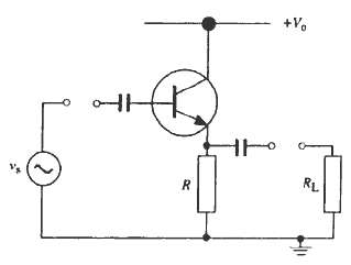
Figure shows a typical low-power npn bipolar transistor of current gain ? = ?I c /?I b
Question:
Figure shows a typical low-power npn bipolar transistor of current gain ? = ?Ic/?Ib, and mutual conductance gm = ?Ic/?Vbe connected for use as an emitter follower. The transistor is fed by an a.c signal from a source of small e.m.f. v1 and negligible impedance, and drives a load of impedance RL. Biassing components are not shown and the impedances of the capacitors can be assumed to be negligible.
(i) Derive expressions for the input impedance of the circuit as seen by the source and the output impedance as seen by the load.
(ii) Derive an expression for the a.c. voltage gain of the circuit and comment on its numerical value.
(iii) Suggest a suitable biassing arrangement and give rough values of the circuit components appropriate for a supply voltage V0 = 9 V and a quiescent emitter current of 1 mA.
Step by Step Answer:
i and ii Since we are dealing with ac signals we can put The emitter current i e is i b i c i b l We can show these currents and voltages on a modifie...View the full answer