

Design a simple MOS current mirror of the type show in Fig. 4.4 to meet the following
Question:
Design a simple MOS current mirror of the type show in Fig. 4.4 to meet the following constraints:
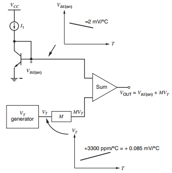
Figure 4.4: Hypothetical band-gap reference circuit
(a) Transistor M2 must operate in the active region for values of VOUT to within 0.2 V of ground.
(b) The output current must be 50 µA.
(c) The output current must change less than 1 percent for a change in output voltage of 1 V.
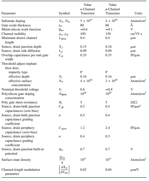
Make M1 and M2 identical. You are to minimize the total device area within the given constraints. Here the device area will be taken to be the total gate area (W × L product). Assume Xd = 0 and take other device data from Table 2.4.
Table 2.4
Fantastic news! We've Found the answer you've been seeking!
Step by Step Answer:
From table 24 K n Cox 450 39 886 10 14 008 10 5 194 AV 2 ...View the full answer

Answered By
Utsab mitra
I have the expertise to deliver these subjects to college and higher-level students. The services would involve only solving assignments, homework help, and others.
I have experience in delivering these subjects for the last 6 years on a freelancing basis in different companies around the globe. I am CMA certified and CGMA UK. I have professional experience of 18 years in the industry involved in the manufacturing company and IT implementation experience of over 12 years.
I have delivered this help to students effortlessly, which is essential to give the students a good grade in their studies.
2+ Reviews
10+ Question Solved
Related Book For 
Analysis and Design of Analog Integrated Circuits
ISBN: 978-0470245996
5th edition
Authors: Paul R. Gray, Paul J. Hurst Stephen H. Lewis, Robert G. Meyer
Question Posted:
