

Question: Using the schematics from Fig. 5.35 and Problem 5.24, design the output stage shown in Fig. 5.32 to satisfy the following requirements. (a) V DD
(a) VDD = VSS = 2.5 V.
(b) The standby power dissipation should be no more than 70 mW.
(c) RL = 100 Ω.
(d) The maximum allowed gain error with zero offsets and all transistors operating in the active region is 1 percent.
(e) In Fig. 5.35,(W/L)17 = (W/L)1/100 and (W/L)13 = (W/L)14 = (W/L)1/10. Similarly, in Problem 5.24, (W/L)27 = (W/L)2/100 and (W/L)23 =(W/L)24 = (W/L)2/10.
(f) To control the quiescent current, the maximum allowed error-amplifier gain is 5.
(g) Your solution is allowed to use four ideal current sources, two in each error amplifier. To allow these ideal current sources to be replaced by real transistors in a design step not required in this problem, the voltage across each ideal current source in Fig. 5.35 must be at least 0.5 V when Vo ‰¥ 0. Similarly, the voltage across each ideal current source in the complementary circuit from Problem 5.24 must be at least 0.5 V when Vo ‰¤ 0.
(h) To guarantee that M16 and M26 do not cut off under these conditions, assume ITAIL = 5 IBIAS in Fig. 5.35 and ITAILP = 5 IBIASP in Problem 5.24.
(i) For both n- and p-channel transistors, assume that λ = 0, Ld = Xd = 0, and ignore the body effect. Use Ldrwn = 1 µm for all transistors, and use Table 2.3 for other transistor parameters.
(j) The distortion of the output stage should be minimized under the above conditions.
Verify your design using SPICE.
Figure 5.35:
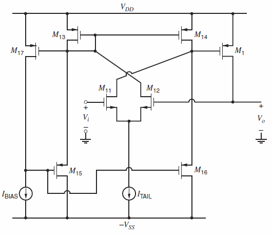
Figure 5.32:
VDD M14 M13 M1 M17 M12 M11 V. M16 M15 O TAIL IBIAS -Vss
Step by Step Solution
3.33 Rating (165 Votes )
There are 3 Steps involved in it
Standby power In Fig 535 I D17 I D13 I D14 flows from V DD to V SS I D1 flows from V DD to M 2 in pr... View full answer

Get step-by-step solutions from verified subject matter experts
Document Format (2 attachments)
1528_605d88e1b35d5_686877.pdf
180 KBs PDF File
1528_605d88e1b35d5_686877.docx
120 KBs Word File