

Question: Using a circuit that is the complement of the one in Fig. 5.35, draw the schematic for the bottom error amplifier and output transistor M
Figure 5.35:
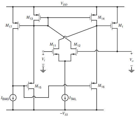
Figure 5.32:
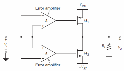
VDD M14 M13 M1 M17 M12 M11 V. M16 M15 O TAIL IBIAS -Vss VDD Error amplifier M1 R13 Vo M2 Error amplifier -Vss Q+
Step by Step Solution
★★★★★
3.48 Rating (161 Votes )
There are 3 Steps involved in it
1 Expert Approved Answer
Step: 1 Unlock

IBIASP M5 M3 M1 VDD Vss ITAILP M2 26 M24 M ... View full answer
Question Has Been Solved by an Expert!
Get step-by-step solutions from verified subject matter experts
Step: 2 Unlock
Step: 3 Unlock
Document Format (2 attachments)
1528_605d88e1b31c7_686876.pdf
180 KBs PDF File
1528_605d88e1b31c7_686876.docx
120 KBs Word File