

Photolithography is an important process in integrated circuit manufacture in which a circuit pattern is transferred from
Question:
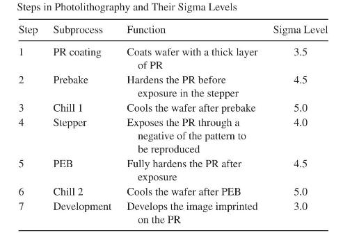
Photolithography is an important process in integrated circuit manufacture in which a circuit pattern is transferred from a mask onto a photosensitive polymer (the PR), ultimately replicating that pattern on the surface of a silicon wafer (Lachman-Shalem et al., 2002). A typical photolithography process consists of seven steps: spin coat of the PR, prebake, chill, expose, post-exposure bake (PEB), chill, and development. The overall objective is to produce printed lines with accurate and consistent width (referred to as the critical dimension, CD). The following table shows the steps required with the sigma level of each step.
(a) Compute the sigma level of the complete process.
(b) You are required to reduce the variance in this process by "process improvements." Given the limited engineering time available, you can allocate only three instances of process improvements, each of which will increase the sigma level of the selected step by 0.5 . Allocate process improvements optimally to maximize the increase in sigma level for the overall process.
Step by Step Answer:


Product And Process Design Principles Synthesis Analysis And Evaluation
ISBN: 9781119355243
4th Edition
Authors: Warren D. Seider, Daniel R. Lewin, J. D. Seader, Soemantri Widagdo, Rafiqul Gani, Ka Ming Ng
