

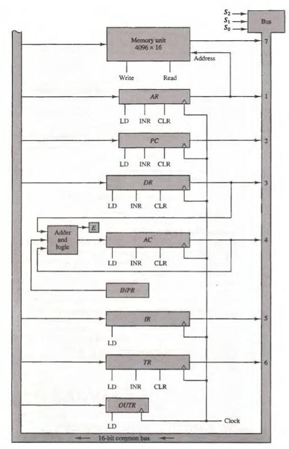
The following register transfers are to be executed in the system of Fig. 5-4. For each transfer,
Question:
The following register transfers are to be executed in the system of Fig. 5-4. For each transfer, specify:
(1) The binary value that must be applied to bus select inputs S2, S1, and S0;
(2) The register whose LD control input must be active (if any);
(3) A memory read or write operation (if needed); and
(4) The operation in the adder and logic circuit (if any).
a. AR←PC
b. IR←M[AR]
c. M[AR]←TR
d. AC←DR, DR←AC (done simultaneously)
Fig. 5-4
Fantastic news! We've Found the answer you've been seeking!
Step by Step Answer:
The following register transfers are to be executed in the system of Fig 54 Here are the details for ...View the full answer

Answered By
PALASH JHANWAR
I am a Chartered Accountant with AIR 45 in CA - IPCC. I am a Merit Holder ( B.Com ). The following is my educational details.
PLEASE ACCESS MY RESUME FROM THE FOLLOWING LINK: https://drive.google.com/file/d/1hYR1uch-ff6MRC_cDB07K6VqY9kQ3SFL/view?usp=sharing
3+ Reviews
10+ Question Solved
Related Book For 
Question Posted:
