All Matches
Solution Library
Expert Answer
Textbooks
Search Textbook questions, tutors and Books
Oops, something went wrong!
Change your search query and then try again
Toggle navigation
FREE Trial
S
Books
FREE
Tutors
Study Help
Expert Questions
Accounting
General Management
Mathematics
Finance
Organizational Behaviour
Law
Physics
Operating System
Management Leadership
Sociology
Programming
Marketing
Database
Computer Network
Economics
Textbooks Solutions
Accounting
Managerial Accounting
Management Leadership
Cost Accounting
Statistics
Business Law
Corporate Finance
Finance
Economics
Auditing
Ask a Question
AI Study Help
New
Search
Search
Sign In
Register
study help
computer science
computer system architecture
Questions and Answers of
Computer System Architecture
Obtain a flowchart for a program to check for a CR code (hexadecimal 0D) in a memory buffer. The buffer contains two characters per word. When the code for CR is encountered, the program transfers it
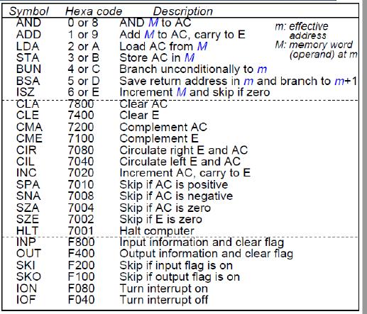
Write a program to unpack two characters from location WRD and store them in bits 0 through 7 of locations CH1 and CH2. Bits 9 through 15 should contain zeros. Symbol Hexa code AND 0 or 8 ADD LDA STA
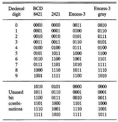
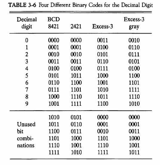
Represent decimal 3984 in the 2421 code of Table 3-6. Complement all bits of the coded number and show that the result is the 9's complement of 3984 in the 2421 code.Table 3-6 Decimal BCD digit 8421
Show the value of all bits of a 12-bit register that hold the number equivalent to decimal 215 in (a) Binary; (b) Binary-coded octal; (c) Binary-coded hexadecimal; (d) Binary-coded decimal (BCD).
Show the bit configuration of a 24-bit register when its content represents the decimal equivalent of 295: (a) In binary; (b) In BCD; (c) In ASCII using eight bits with even parity.
Write your name in ASCII using an 8-bit code with the leftmost bit always 0. Include a space between names and a period after a middle initial.
Decode the following ASCII code: 1001010 1001111 1001000 1001110 0100000 1000100 1001111 1000101
Obtain the 9's complement of the following eight-digit decimal numbers: 12349876; 00980100; 90009951; and 00000000.
Obtain the 10's complement of the following six-digit decimal numbers: 123900; 090657; 100000; and 000000.
Obtain the 1's and 2's complements of the following eight-digit binary numbers: 10101110; 10000001; 10000000; 00000001; and 00000000.
Perform the subtraction with the following unsigned decimal numbers by taking the 10's complement of the subtrahend. a. 5250 - 1321 b. 1753-8640c. 20-100 d.
Perform the subtraction with the following unsigned binary numbers by taking the 2's complement of the subtrahend. a. 1101010000 b. 110101101c. 100 - 110000 d. 10101001010100
Perform the arithmetic operations (+42) + (-13) and (-42) - (-13) in binary using signed-2's complement representation for negative numbers.
Perform the arithmetic operations (+70) + (+80) and (-70) + (-80) with binary numbers in signed-2's complement representation. Use eight bits to accommodate each number together with its sign. Show
Perform the following arithmetic operations with the decimal numbers using signed-10's complement representation for negative numbers. a. (-638) + (+785) b. (-638) (+185)
A 36-bit floating-point binary number has eight bits plus sign for the exponent and 26 bits plus sign for the mantissa. The mantissa is a normalized fraction. Numbers in the mantissa and exponent are
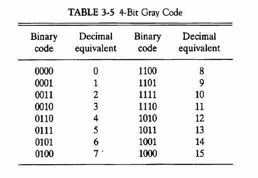
The Gray code is sometimes called a reflected code because the bit values are reflected on both sides of any 2" value. For example, as shown in Table 3-5, the values of the three low-order bits are
Represent the number (+46.5)10 as a floating-point binary number with 24 bits. The normalized fraction mantissa has 16 bits and the exponent has 8 bits.
Represent decimal number 8620 in (a) BCD; (b) Excess-3 code; (c) 2421 code; (d) As a binary number.
List the 10 BCD digits with an even parity in the leftmost position (total of five bits per digit). Repeat with an odd-parity bit.
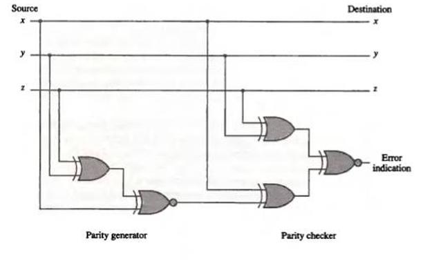
Derive the circuits for a 3-bit parity generator and 4-bit parity checker using an even-parity bit. (The circuits of Fig. 3-3 use odd parity.)Fig. 3-3 Source X Parity generator Parity
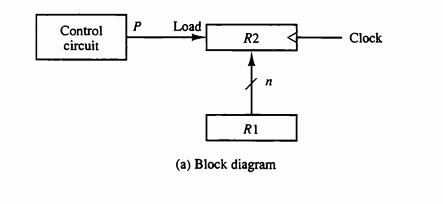
Show the block diagram of the hardware (similar to Fig. 4-2a) that implements the following register transfer statement: yT2: R2 ← R1, R1← R2Fig. 4-2(a) Control circuit P Load R2 R1 n (a) Block
Show that the exclusive-OR function x = A ⊕ B ⊕ C ⊕ D is an odd function. One way to show this is to obtain the truth table for y = A ⊕ B and for z = C ⊕ D and then formulate the truth
The outputs of four registers, R0, R1, R2, and R3, are connected through 4-to-1-line multiplexers to the inputs of a fifth register, R5. Each register is eight bits long. The required transfers are
Represent the following conditional control statement by two register transfer statements with control functions. If (P = 1) then (R1←R2) else if (Q = 1) then (R1←R3)
What has to be done to the bus system of Fig. 4-3 to be able to transfer information from any register to any other register? Specifically, show the connections that must be included to provide a
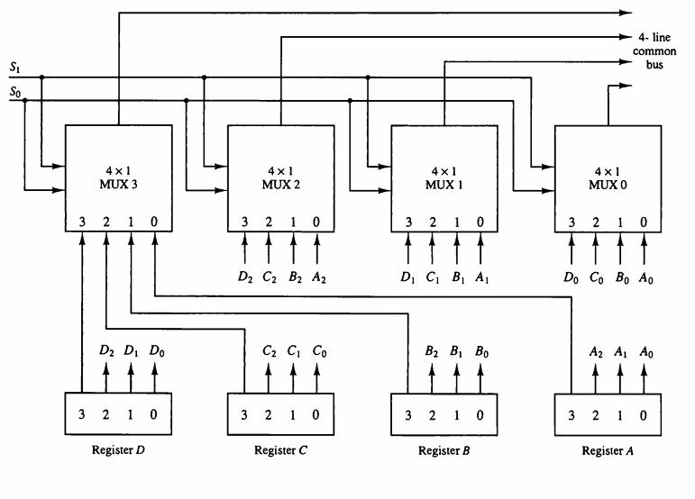
Draw a diagram of a bus system similar to the one shown in Fig. 4-3, but use three-state buffers and a decoder instead of the multiplexers.Fig. 4-3 S₁ So 4x1 MUX 3 3 2 1 0 D₂ D₁ Do 3 2
A digital computer has a common bus system for 16 registers of 32 bits each. The bus is constructed with multiplexers. a. How many selection inputs are there in each multiplexer? b. What size of
Show the hardware that implements the following statement. Include the logic gates for the control function and a block diagram for the binary counter with a count enable input.xyT0 + T1+ y'T2:
Consider the following register transfer statements for two 4-bit registers R1 and R2. xT: R1←R1 + R2 x'T: R1←R2Every time that variable T = 1, either the content of R2 is added to the
Using a 4-bit counter with parallel load as in Fig. 2-11 and a 4-bit adder as in Fig. 4-6, draw a block diagram that shows how to implement the following statements: x :R1←R1 + R2 Add
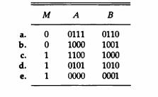
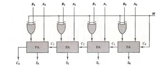
The adder-subtractor circuit of Fig. 4-7 has the following values for input mode M and data inputs A and B. In each case, determine the values of the outputs: S3, S2, S1, S0, and C4.Fig. 4-7
Draw the block diagram for the hardware that implements the following statements: x + yz: AR←AR + BR where AR and BR are two n-bit registers and x, y, and z are control variables. Include the
The following transfer statements specify a memory. Explain the memory operation in each case. a. R2←M[AR] b. M[AR]←R3 c. R5←M[R5]
Design a 4-bit combinational circuit decrementer using four full-adder circuits.
Design an arithmetic circuit with one selection variable S and two n-bit data inputs A and B. The circuit generates the following four arithmetic operations in conjunction with the input carry Cin.
Derive a combinational circuit that selects and generates any of the 16 logic functions listed in Table 4-5.Table 4-5 x y Fo F₁ F₂ F3 1000 00 0 1 1 TABLE 4-5 Truth Tables for 16 Functions of Two
Design a digital circuit that performs the four logic operations of exclusive-OR, exclusive-NOR, NOR, and NAND. Use two selection variables. Show the logic diagram of one typical stage.
The 8-bit registers AR, BR, CR, and DR initially have the following values: AR= 11110010 BR = 11111111 CR = 10111001 DR = 11101010 Determine the 8-bit values in each register after the execution
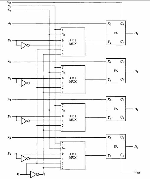
Assume that the 4-bit arithmetic circuit of Fig. 4-9 is enclosed in one IC package. Show the connections among two such ICs to form an 8-bit arithmetic circuit.Fig. 4-9
Explain why each of the following microoperations cannot be executedduring a single clock pulse in the system shown in Fig. 5-4. Specify a sequence of microoperations that will perform the
Determine by means of a truth table the validity of DeMorgan's theorem for three variables: (ABC)' = A' + B' + C'.
List the truth table of a three-variable exclusive-OR (odd) function: x = A ⊕ B ⊕ C.
Simplify the following expressions using Boolean algebra. a. A + AB b. AB + AB' c. A'BC + AC d. A'B + ABC' + ABC
Simplify the following expressions using Boolean algebra. a. AB + A(CD + CD') b. (BC' + A'D) (AB' + CD')
Using DeMorgan's theorem, show that: a. (A + B)'(A' + B')' = 0 b. A + A'B + A'B' = 1
Given the Boolean expression F= x'y + xyz': a. Derive an algebraic expression for the complement F'. b. Show that F-F' = 0. c. Show that F + F' = 1.
Given the Boolean function F = xyz + x'y'z + xyz a. List the truth table of the function. b. Draw the logic diagram using the original Boolean expression. c. Simplify the algebraic expression
Simplify the following Boolean functions using three-variable maps. a. F(x, y, z) = ∑ (0,1,5,7) b. F(x, y, z) = ∑ (1,2,3,6,7)c. F(x, y, z) = ∑ (3,5,6,7) d. F(A, B, C) = ∑ (0,2,3,4.6)
Simplify the following Boolean functions using four-variable maps. a. F(A, B, C, D) = ∑ (4,6,7,15) b. F(A, B, C, D) = ∑ (3, 7, 11, 13, 14, 15)c. F(A, B, C, D) = ∑ (0, 1, 2, 4, 5, 7, 11, 15)d.
Simplify the following expressions in (1) sum-of-products form and (2) product-of-sums form. a. x'z' + y'z' + yz' + xy b. AC' + B'D + A'CD + ABCD
Simplify the following Boolean function in sum-of-products form by means of a four-variable map. Draw the logic diagram with (a) AND-OR gates; (b) NAND gates. F(A, B, C, D) = ∑ (0, 2, 8, 9, 10,
Simplify the following Boolean function in product-of-sums form by means of a four-variable map. Draw the logic diagram with (a) OR-AND gates; (b) NOR gates. F(w, x, y, z) = ∑ (2, 3, 4, 5, 6, 7,
Simplify the Boolean function F together with the don't-care conditions d in (1) Sum-of-products form;(2) Product-of-sums form. F(w, x, y, z) = ∑ (0, 1, 2, 3, 7, 8, 10)d(w, x, y, z) = ∑ (5, 6,
Using Table 1-2, derive the Boolean expression for the S (sum) output of the full-adder in sum-of-products form. Then by algebraic manipulation show that S can be expressed as the exclusive-OR of the
A majority function is generated in a combinational circuit when the output is equal to 1 if the input variables have more I's than 0's. The output is 0 otherwise. Design a three-input majority
Design a combinational circuit with three inputs x, y, z and three outputs A, B, C. When the binary input is 0, 1, 2, or 3, the binary output is one greater than the input. When the binary input is
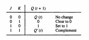
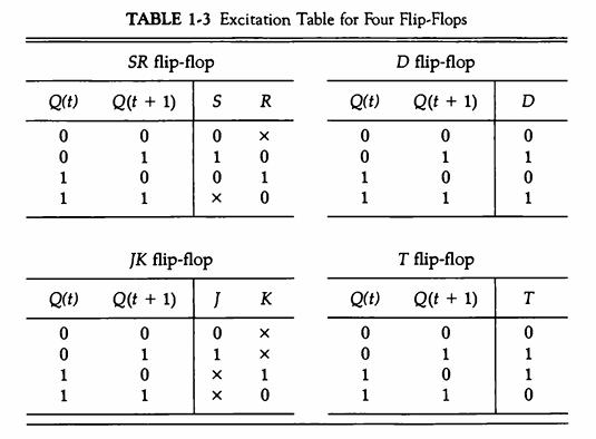
Using the information from the characteristic table of the JK flip-flop listed in Fig. 1-21(b), derive the excitation table for the JK flip-flop and compare your answer with Table 1-3.Fig.
Show that a JK flip-flop can be converted to a D flip-flop with an inverter between the J and K inputs.
A sequential circuit has two D flip-flops A and B, two inputs x and y, and one output z. The flip-flop input equations and the circuit output are as follows: DA = x'y + xA DB = x'B + xA z = Ba.
Design a 2-bit count-down counter. This is a sequential circuit with two flip-flops and one input x. When x = 0, the state of the flip-flops does not change. When x = 1, the state sequence is 11, 10,
Design a sequential circuit with two JK flip-flops A and B and two inputs E and x. If E = 0, the circuit remains in the same state regardless of the value of x. When E = 1 and x = 1, the circuit goes
TTL SSI come mostly in 14-pin IC packages. Two pins are reserved for power supply and the other pins are used for input and output terminals. How many circuits are included in one such package if it
MSI chips perform elementary digital functions such as decoders, multiplexers, registers, and counters. The following are TTL-type integrated circuits that provide such functions. Find their
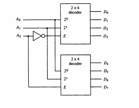
Construct a 5-to-32-line decoder with four 3-to-8-line decoders with enable and one 2-to-4-line decoder. Use block diagrams similar to Fig. 2-3.Fig. 2-3
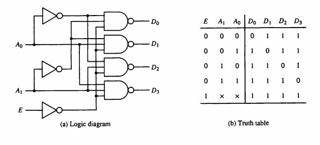
Modify the decoder of Fig. 2-2 so that the circuit is enabled when E = 1and disabled when E = 0. List the modified truth table.Fig. 2-2 Ao A₁ E Da Do- (a) Logic diagram Do D₁ -D₂ D3 E A₁ Ao
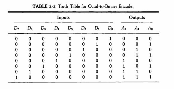
Draw the logic diagram of an eight-input, three-output encoder whose truth table is given in Table 2-2. What is the output when all the inputs are equal to 0? What is the output when only input Do is
Draw the logic diagram of a 2-to-4-line decoder with only NOR gates. Include an enable input.
Construct a 16-to-1-line multiplexer with two 8-to-1-line multiplexers and one 2-to-1-line multiplexer. Use block diagrams for the three multiplexers.
Include a two-input AND gate with the register of Fig. 2-6 and connect the gate output to the clock inputs of all the flip-flops. One input of the AND gate receives the clock pulses from the clock
Draw the block diagram of a dual 4-to-1-line multiplexers and explain its operation by means of a function table.
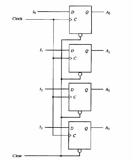
What is the purpose of the buffer gate in the clock input of the register of Fig. 2-7?Fig. 2-7 Clock Clear To 4 1₂2 1₂ D C D DC с D C D C e e e e A A₁ A₂ A3
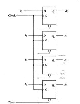
Include a synchronous clear capability to the register with parallel load of Fig. 2-7.Fig. 2-7 Clock Clear lo 4 1₂2 13 D C D DC с D C D e e e e A A₁ A₂ 102 tini 43 1
The content of a 4-bit register is initially 1101. The register is shifted six times to the right with the serial input being 101101. What is the content of the register after each shift?
A ring counter is a shift register as in Fig. 2-8 with the serial output connected to the serial input. Starting from an initial state of 1000, list the sequence of states of the four flip-flops
What is the difference between serial and parallel transfer? Using a shift register with parallel load, explain how to convert serial input data to parallel output and parallel input data to serial
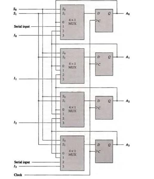
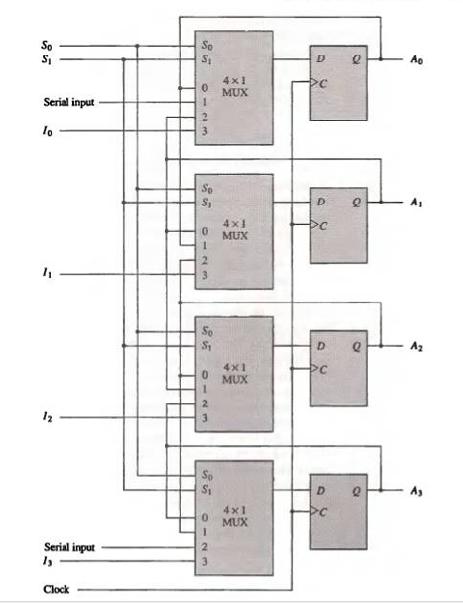
The 4-bit bidirectional shift register with parallel load shown in Fig. 2-9 is enclosed within one IC package. a. Draw a block diagram of the IC showing all inputs and outputs. Include two pins for
How many flip-flops will be complemented in a 10-bit binary counter to reach the next count after (a) 1001100111; (b) 0011111111?
Show the connections between four 4-bit binary counters with parallel load (Fig. 2-11) to produce a 16-bit binary counter with parallel load. Use a block diagram for each 4-bit counter.Fig. 2-11
Show how the binary counter with parallel load of Fig. 2-11 can be made to operate as a divide-by-N counter (i.e., a counter that counts from 0000 to N-and back to 0000). Specifically show the
The following memory units are specified by the number of words times the number of bits per word. How many address lines and input-output data lines are needed in each case? (a) 2K x 16; (b) 64K x
Specify the number of bytes that can be stored in the memories listed in Prob. 2-19.Prob. 2-19The following memory units are specified by the number of words times the number of bits per word. How
How many 128 x 8 memory chips are needed to provide a memory capacity of 4096 x 16?
Given a 32 x 8 ROM chip with an enable input, show the external connections necessary to construct a 128 x 8 ROM with four chips and a decoder.
A ROM chip of 4096 x 8 bits has two enable inputs and operates from a 5-volt power supply. How many pins are needed for the integrated circuit package? Draw a block diagram and label all input and
Convert the following binary numbers to decimal: 101110; 1110101; and 110110100.
Convert the following numbers with the indicated bases to decimal: (12121)3; (4310)5; (50)7; and (198)12.
Convert the following decimal numbers to binary: 1231; 673; and 1998.
Convert the following decimal numbers to the bases indicated. a. 7562 to octal b. 1938 to hexadecimal c. 175 to binary
Convert the hexadecimal number F3A7C2 to binary and octal.
What is the radix of the numbers if the solution to the quadratic equation x10x + 31 = 0 is x = 5 and x = 8?
What are the two instructions needed in the basic computer in order to set the E flip-flop to 1?
The content of AC in the basic computer is hexadecimal A937 and the initial value of E is 1. Determine the contents of AC, E, PC, AR, and IR in hexadecimal after the execution of the CLA instruction.
Register A holds the 8-bit binary 11011001. Determine the B operand and the logic microoperation to be performed in order to change the value in A to: a. 01101101 b. 11111101
An 8-bit register contains the binary value 10011100. What is the register value after an arithmetic shift right? Starting from the initial number 10011100, determine the register value after an
Starting from an initial value of R = 11011101, determine the sequence of binary values in R after a logical shift-left, followed by a circular shift-right, followed by a logical shift-right and a
A computer uses a memory unit with 256K words of 32 bits each. A binary instruction code is stored in one word of memory. The instruction has four parts: an indirect bit, an operation code, a
What is the difference between a direct and an indirect address instruction? How many references to memory are needed for each type of instruction to bring an operand into a processor register?
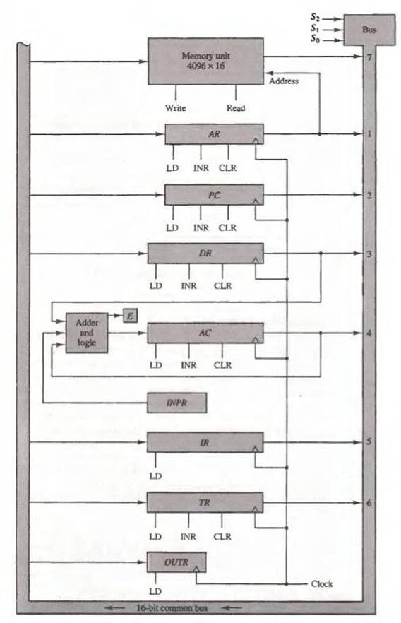
The following control inputs are active in the bus system shown in Fig. 5-4. For each case, specify the register transfer that will be executed during the next clock transition.Fig. 5-4
The following register transfers are to be executed in the system of Fig. 5-4. For each transfer, specify: (1) The binary value that must be applied to bus select inputs S2, S1, and S0; (2) The
Showing 1 - 100
of 331
1
2
3
4