

Question: Consider the following circuit where the combinational circuit is represented by COMB and clock skew is represented by tskew. Given the following parameters: FF setup
Given the following parameters:
FF setup time = 10 ns
FF hold time = 2 ns
FF propagation delay = 12 to 20 ns
Tcomb1 = 5 ns to 7 ns
Tcomb2 = 6 ns to 11 ns
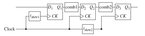
(a) What is the minimum clock period with tskew1 = 0; tskew2 = 3?
(b) Now set Tcomb1 = 1 to 4 ns. Is there a setup time violation for the middle flip-flop? If no, what is the setup time margin?
(c) Now set Tcomb1 = 1 to 4 ns. Is there a hold-time violation for the middle flip-flop? If no, what is the hold-time margin?
(d) What are the minimum values of tskew1 and tskew2 that will fix the violations?
(e) What is the minimum clock period after violations have been fixed?
D QHcomb1-D2 Q2Hcomb2HD3 Q3 fskewl CK CK CK Clock skew2
Step by Step Solution
3.51 Rating (178 Votes )
There are 3 Steps involved in it
a Consider following delays The maximum of these is 38 ns Therefore the ... View full answer

Get step-by-step solutions from verified subject matter experts