

Question: Redesign the floating-point multiplier in Figure 7. 7 using a common 5-bit full adder connected to a bus instead of two separate adders for the
(a) Redraw the block diagram, being sure to include the connections to the bus, and include all control signals.
(b) Draw a new SM chart for the new control.
(c) Write the Verilog description for the multiplier or specify the changes that need to be made to an existing description.
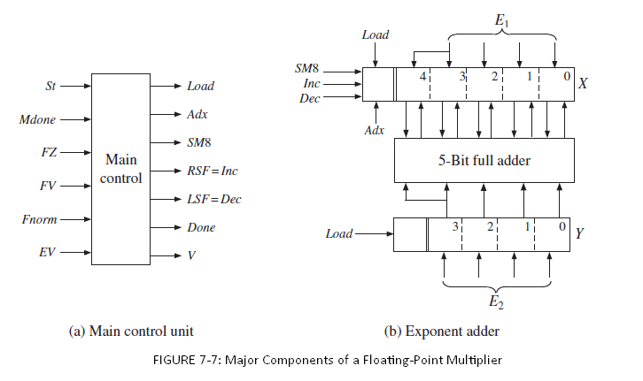
E1 Load SM8 2 Inc- St Load Dec Adx Mdone Adx SM8 FZ Main 5-Bit full adder RSF=Inc control FV LSF= Dec Fnorm 3 2 Done Load EV E2 (a) Main control unit (b) Exponent adder FIGURE 7-7: Major Components of a Floating-Point Multiplier 4.
Step by Step Solution
★★★★★
3.48 Rating (164 Votes )
There are 3 Steps involved in it
1 Expert Approved Answer
Step: 1 Unlock

a b SM chart is similar to Figure 78 with added states for loading c define M B 0 module Prob711 CLK St Input Fout Eout V Done input CLK St input 3 0 ... View full answer
Question Has Been Solved by an Expert!
Get step-by-step solutions from verified subject matter experts
Step: 2 Unlock
Step: 3 Unlock