

Question: (a) For the ASM chart derived in Problem 7.1, show another ASM chart that specifies the required control signals to control the datapath circuit. Assume
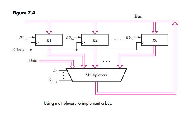
(a) For the ASM chart derived in Problem 7.1, show another ASM chart that specifies the required control signals to control the datapath circuit. Assume that multiplexers are used to implement the bus that connects the registers, as shown in Figure 7.4.(b)Write complete Verilog code for the system in Problem 7.1, including the control circuit described in part (a).(c) Synthesize a circuit from the Verilog code written in part (b) and show a timing simulation that illustrates correct functionality of the circuit.
Data From Problem 7.1
In Section 7.1 we showed a digital system with three registers, R1 to R3, and we designed a control circuit that can be used to swap the contents of registers R1 and R2. Give an ASM chart that represents this digital system and the swap operation.
Data From Section 7.1
Outputs of two ordinary logic gates cannot be connected together, because a short circuit would result if one gate forces the output value 1 while the other gate forces the value 0. Therefore, some special gates are needed if the outputs of two registers are to be connected to a common set of wires. A commonly used circuit element for this purpose is shown in Figure 7.1a. It has a data input w, an output f, and an enable input e. Its operation is illustrated by the equivalent circuit in part (b). The triangular symbol in the figure represents a noninverting driver, which is a circuit that performs no logic operation and its output simply replicates the input signal. Its purpose is to provide additional electrical driving capability. In conjunction with the output switch, it behaves as indicated in Figure 7.1c. When e = 1, the output reflects the logic value on the data input. But, when e = 0, the output is electrically disconnected from the data input, which is referred to as a high impedance state and it is usually denoted by the letter Z (or z). Because this circuit element exhibits three distinct states, 0, 1, and Z, it is called a tri-state driver (or buffer). Appendix B explains how it can be implemented with transistors.
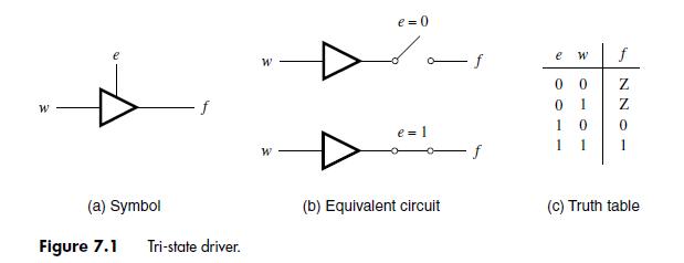
W (a) Symbol Figure 7.1 Tri-state driver. W W e=0) e = 1 (b) Equivalent circuit f e W f 0 0 01 0 1 1 1 NN 1 (c) Truth table
Step by Step Solution
3.31 Rating (160 Votes )
There are 3 Steps involved in it
Description The saturation domes for R134a and isopentane shown i... View full answer

Get step-by-step solutions from verified subject matter experts