

Question: 1. A Si step junction under equilibrium at 300 K has the following doping characteristics: NA = 5x105 cm- ND 1 x 105 cm-3
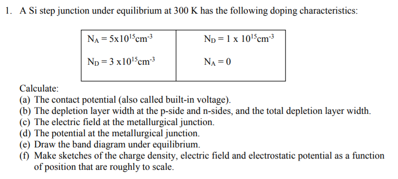
1. A Si step junction under equilibrium at 300 K has the following doping characteristics: NA = 5x105 cm- ND 1 x 105 cm-3 ND= 3 x105 cm- NA = 0 Calculate: (a) The contact potential (also called built-in voltage). (b) The depletion layer width at the p-side and n-sides, and the total depletion layer width. (c) The electric field at the metallurgical junction. (d) The potential at the metallurgical junction. (e) Draw the band diagram under equilibrium. (f) Make sketches of the charge density, electric field and electrostatic potential as a function of position that are roughly to scale.
Step by Step Solution
3.47 Rating (157 Votes )
There are 3 Steps involved in it

Get step-by-step solutions from verified subject matter experts