

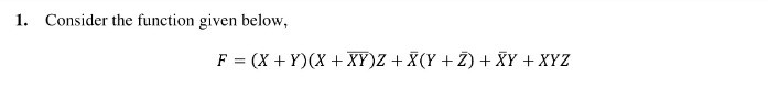
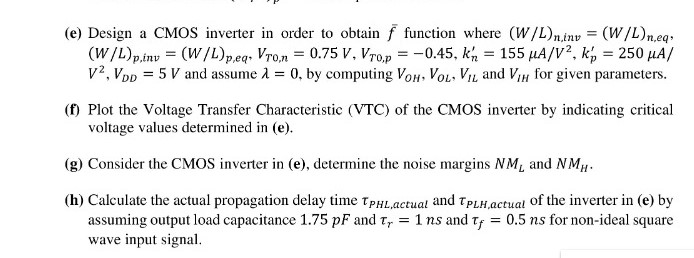
Question: 1. Consider the function given below, F = (X+Y)(X + XY)2 + X(Y + 2) + XY + XYZ (e) Design a CMOS inverter in
1. Consider the function given below, F = (X+Y)(X + XY)2 + X(Y + 2) + XY + XYZ (e) Design a CMOS inverter in order to obtain f function where (W/L) n.inv = (W/L) n,eq, (W/L)p,inv = (W/L)p.eq, Vron = 0.75 V, VTO,p = -0.45, k = 155 mA/V2, k, = 250 LA/ V2, Vpp = 5 V and assume 1 = 0, by computing Vow, VOL. VIL and V/for given parameters. (f) Plot the Voltage Transfer Characteristic (VTC) of the CMOS inverter by indicating critical voltage values determined in (e). (g) Consider the CMOS inverter in (e), determine the noise margins NM and NM, (h) Calculate the actual propagation delay time Tphl,actual and Tply,actual of the inverter in (e) by assuming output load capacitance 1.75 pF and T, = 1 ns and tp = 0.5 ns for non-ideal square wave input signal. 1. Consider the function given below, F = (X+Y)(X + XY)2 + X(Y + 2) + XY + XYZ (e) Design a CMOS inverter in order to obtain f function where (W/L) n.inv = (W/L) n,eq, (W/L)p,inv = (W/L)p.eq, Vron = 0.75 V, VTO,p = -0.45, k = 155 mA/V2, k, = 250 LA/ V2, Vpp = 5 V and assume 1 = 0, by computing Vow, VOL. VIL and V/for given parameters. (f) Plot the Voltage Transfer Characteristic (VTC) of the CMOS inverter by indicating critical voltage values determined in (e). (g) Consider the CMOS inverter in (e), determine the noise margins NM and NM, (h) Calculate the actual propagation delay time Tphl,actual and Tply,actual of the inverter in (e) by assuming output load capacitance 1.75 pF and T, = 1 ns and tp = 0.5 ns for non-ideal square wave input signal
Step by Step Solution
There are 3 Steps involved in it

Get step-by-step solutions from verified subject matter experts