

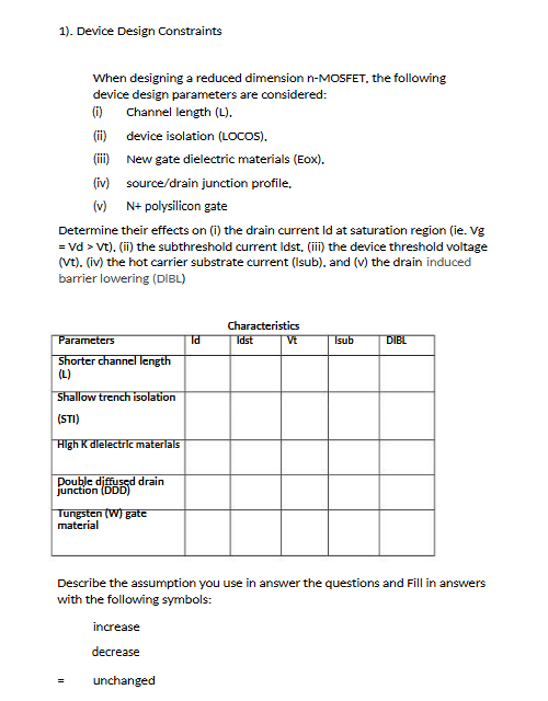
Question: 1 ) . Device Design Constraints When designing a reduced dimension n - MOSFET, the following device design parameters are considered: ( i ) Channel
Device Design Constraints
When designing a reduced dimension nMOSFET, the following device design parameters are considered:
i Channel length L
ii device isolation LOCOS
iii New gate dielectric materials Eox
iv sourcedrain junction profile.
vmathrmN polysilicon gate
Determine their effects on i the drain current ld at saturation region ie Vg mathrmVdmathrmVtii the subthreshold current ldstiii the device threshold voltage Vtiv the hot carrier substrate current lsub and v the drain induced barrier lowering DIBL
Characteristics
begintabularllllll
hline Parameters & Id & ldst & Vt & lsub & DIBL
hline begintabularl
Shorter channel length
L
endtabular & & & & &
hline begintabularl
Shallow trench isolation
STI
endtabular & & & & &
hline High K dlelectric materlals & & & & &
hline begintabularl
pouble diffused drain
junction DDD
endtabular & & & & &
hline begintabularl
Tungsten W gate
material
endtabular & & & & &
hline
endtabular
Describe the assumption you use in answer the questions and Fill in answers with the following symbols:
increase
decrease
unchanged
Step by Step Solution
There are 3 Steps involved in it
1 Expert Approved Answer
Step: 1 Unlock

Question Has Been Solved by an Expert!
Get step-by-step solutions from verified subject matter experts
Step: 2 Unlock
Step: 3 Unlock