

Question: 1 . For ( 1 3 0 - mathrm { nm } ) CMOS node, 2 nm of SiON is used as
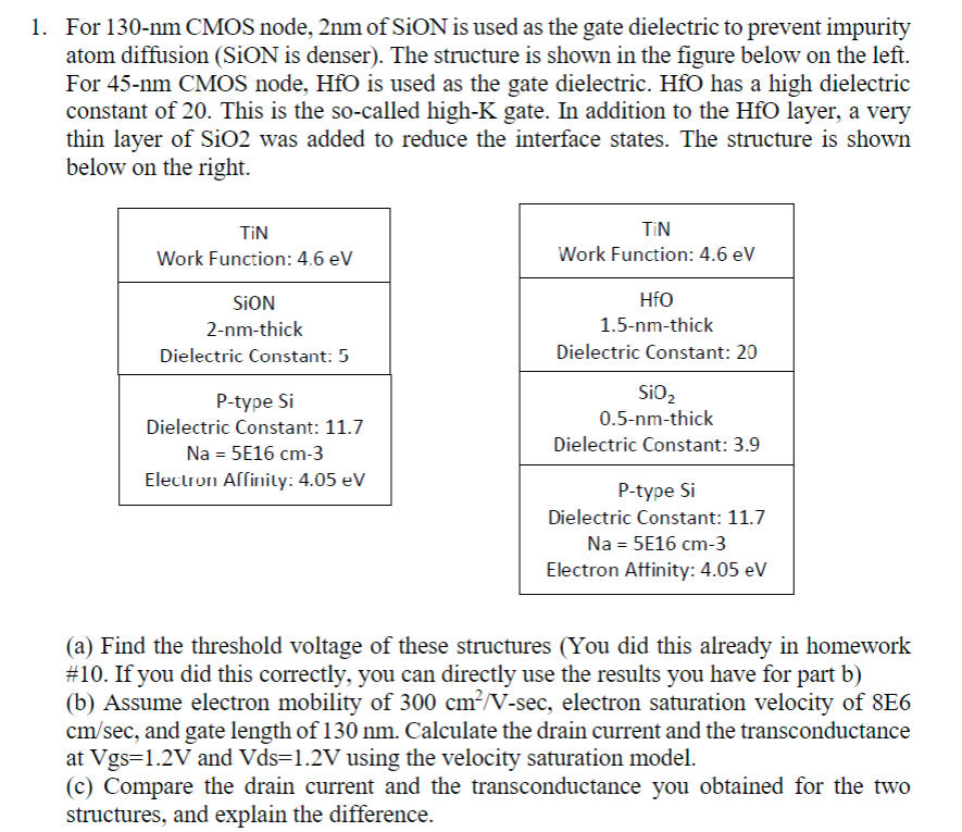
For mathrmnm CMOS node, nm of SiON is used as the gate dielectric to prevent impurity atom diffusion SiON is denser The structure is shown in the figure below on the left. For mathrmnm CMOS node, HfO is used as the gate dielectric. HfO has a high dielectric constant of This is the socalled highK gate. In addition to the HfO layer, a very thin layer of SiO was added to reduce the interface states. The structure is shown below on the right.
a Find the threshold voltage of these structures You did this already in homework # If you did this correctly, you can directly use the results you have for part bb Assume electron mobility of mathrm~cmmathrmVsec electron saturation velocity of Emathrmcmmathrmsec and gate length of nm Calculate the drain current and the transconductance at mathrmVgsmathrm~V and mathrmVdsmathrm~V using the velocity saturation model.
c Compare the drain current and the transconductance you obtained for the two structures, and explain the difference.
Step by Step Solution
There are 3 Steps involved in it
1 Expert Approved Answer
Step: 1 Unlock

Question Has Been Solved by an Expert!
Get step-by-step solutions from verified subject matter experts
Step: 2 Unlock
Step: 3 Unlock