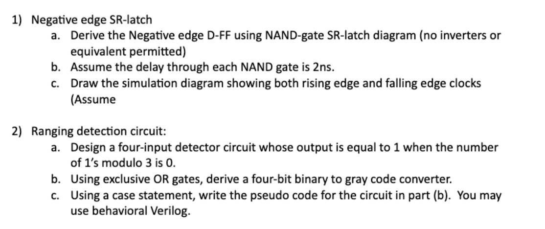
Question: 1 ) Negative edge SR - latch a . Derive the Negative edge D - FF using NAND - gate SR - latch diagram (
Negative edge SRlatch
a Derive the Negative edge DFF using NANDgate SRlatch diagram no inverters or equivalent permitted
b Assume the delay through each NAND gate is ns
c Draw the simulation diagram showing both rising edge and falling edge clocks Assume
Ranging detection circuit:
a Design a fourinput detector circuit whose output is equal to when the number of s modulo is
b Using exclusive OR gates, derive a fourbit binary to gray code converter.
c Using a case statement, write the pseudo code for the circuit in part b You may use behavioral Verilog.

Step by Step Solution
There are 3 Steps involved in it
1 Expert Approved Answer
Step: 1 Unlock


Question Has Been Solved by an Expert!
Get step-by-step solutions from verified subject matter experts
Step: 2 Unlock
Step: 3 Unlock


