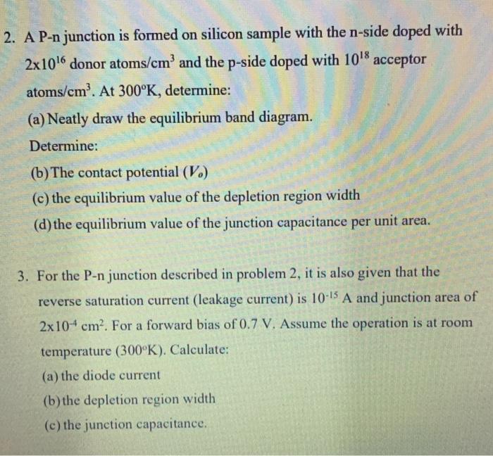
Question: 2. A P-n junction is formed on silicon sample with the n-side doped with 2x10donor atoms/cm' and the p-side doped with 10 acceptor atoms/cm. At

2. A P-n junction is formed on silicon sample with the n-side doped with 2x10donor atoms/cm' and the p-side doped with 10" acceptor atoms/cm. At 300K, determine: (a) Neatly draw the equilibrium band diagram. Determine: (b) The contact potential (V.) (c) the equilibrium value of the depletion region width (d) the equilibrium value of the junction capacitance per unit area. 3. For the P-n junction described in problem 2, it is also given that the reverse saturation current (leakage current) is 10-15 A and junction area of 2x10 cm. For a forward bias of 0.7 V. Assume the operation is at room temperature (300K). Calculate: (a) the diode current (b) the depletion region width (c) the junction capacitance
Step by Step Solution
There are 3 Steps involved in it

Get step-by-step solutions from verified subject matter experts


