

Question: (2) Design a combinational circuit for 8-bit BCD to binary conversion. Name the design as bcd_2_bin. The interface of the design and its function are
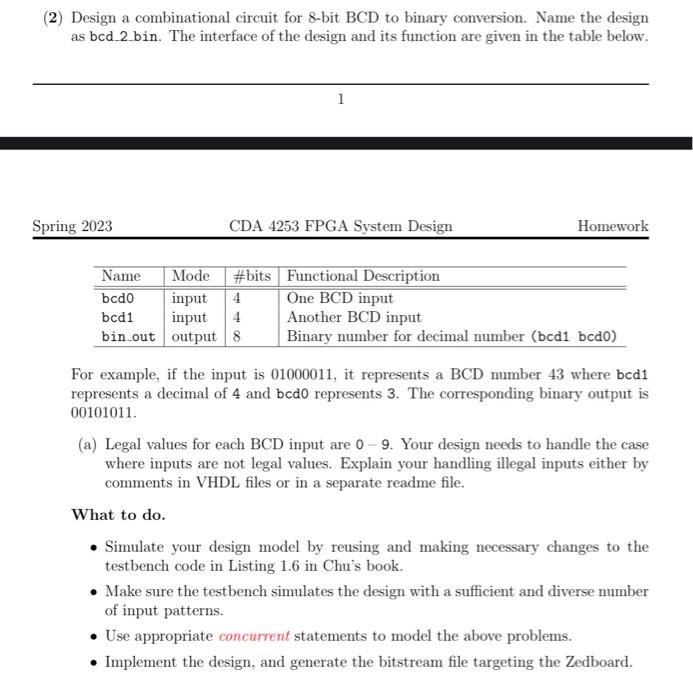
(2) Design a combinational circuit for 8-bit BCD to binary conversion. Name the design as bcd_2_bin. The interface of the design and its function are given in the table below. 1 Spring 2023 CDA 4253 FPGA System Design Homework For example, if the input is 01000011 , it represents a BCD number 43 where bcd1 represents a decimal of 4 and bcd0 represents 3 . The corresponding binary output is 00101011. (a) Legal values for each BCD input are 0 - 9. Your design needs to handle the case where inputs are not legal values. Explain your handling illegal inputs either by comments in VHDL files or in a separate readme file. What to do. - Simulate your design model by reusing and making necessary changes to the testbench code in Listing 1.6 in Chu's book. - Make sure the testbench simulates the design with a sufficient and diverse number of input patterns. - Use appropriate concurrent statements to model the above problems. - Implement the design, and generate the bitstream file targeting the Zedboard
Step by Step Solution
There are 3 Steps involved in it

Get step-by-step solutions from verified subject matter experts