

Question: 2. Part A. Convert the circuit below into NAND gates. Insert or re necessary. both the original Part B. What is the propagation delay from
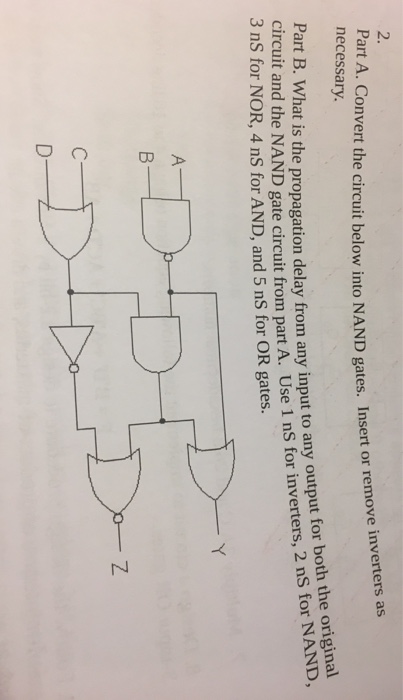
2. Part A. Convert the circuit below into NAND gates. Insert or re necessary. both the original Part B. What is the propagation delay from any input to any output for s for NAND, circuit and the NAND gate circuit from part A. Use 1 nS for inverters, 2 n 3 nS for NOR, 4 nS for AND, and 5 nS for OR gates
Step by Step Solution
There are 3 Steps involved in it
1 Expert Approved Answer
Step: 1 Unlock

Question Has Been Solved by an Expert!
Get step-by-step solutions from verified subject matter experts
Step: 2 Unlock
Step: 3 Unlock