

Question: 3. Consider the gate-level circuit in the figure. (a) Determine the function of the circuit. [ AB] (b) Draw an equivalent complementary CMOS transistor circuit.
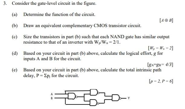
3. Consider the gate-level circuit in the figure. (a) Determine the function of the circuit. [ AB] (b) Draw an equivalent complementary CMOS transistor circuit. (c) Size the transistors in part (b) such that each NAND gate has similar output resistance to that of an inverter with W/W.= 2/1. [W, =W. 2] (d) Based on your circuit in part (b) above, calculate the logical effort, g for inputs A and B for the circuit. [ga-gu= 4/3] (e) Based on your circuit in part (b) above, calculate the total intrinsic path delay, P=Ep; for the circuit. [p = 2, P=6] BE
Step by Step Solution
There are 3 Steps involved in it
1 Expert Approved Answer
Step: 1 Unlock

Question Has Been Solved by an Expert!
Get step-by-step solutions from verified subject matter experts
Step: 2 Unlock
Step: 3 Unlock