

Question: 3 This question is about Digital Logic (5) PPUCS (a) Show, using a diagram, how you could construct a half-adder from boolean logic gates. (b)
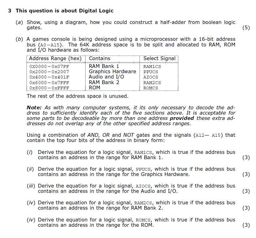
3 This question is about Digital Logic (5) PPUCS (a) Show, using a diagram, how you could construct a half-adder from boolean logic gates. (b) A games console is being designed using a microprocessor with a 16-bit address bus (A0-A15). The 64K address space is to be split and allocated to RAM, ROM and I/O hardware as follows: Address Range (hex) Contains Select Signal OX0000 - 0x07FF RAM Bank 1 RAMICS 0x2000-0x2007 Graphics Hardware Ox4000-0x401F Audio and I/O AIOCS Ox6000-0x7FFF RAM Bank 2 RAM2CS Ox8000-OxFFFF ROM ROMCS The rest of the address space is unused. Note: As with many computer systems, it its only necessary to decode the ad- dress to sufficiently identify each of the five sections above. It is acceptable for some parts to be decodeable by more than one address provided these extra ad- dresses do not overlap any of the other specified address ranges. Using a combination of AND, OR and NOT gates and the signals (A12- A15) that contain the top four bits of the address in binary form: (1) Derive the equation for a logic signal, RAMICS, which is true if the address bus contains an address in the range for RAM Bank 1. (ii) Derive the equation for a logic signal, PPUCS, which is true if the address bus contains an address in the range for the Graphics Hardware. (iii) Derive the equation for a logic signal, AIOCS, which is true if the address bus contains an address in the range for the Audio and I/O. (iv) Derive the equation for a logic signal, RAM2Cs, which is true if the address bus contains an address in the range for RAM Bank 2. (3) (3) (3) (3) (iv) Derive the equation for a logic signal, ROMCS, which is true if the address bus contains an address in the range for the ROM. (3)
Step by Step Solution
There are 3 Steps involved in it

Get step-by-step solutions from verified subject matter experts