

Question: 4 . 5 Voltage - Divider Bias Figure 4 . 5 depicts the voltage - divider bias circuit for an n - channel enhancementmode MOSFET,
VoltageDivider Bias
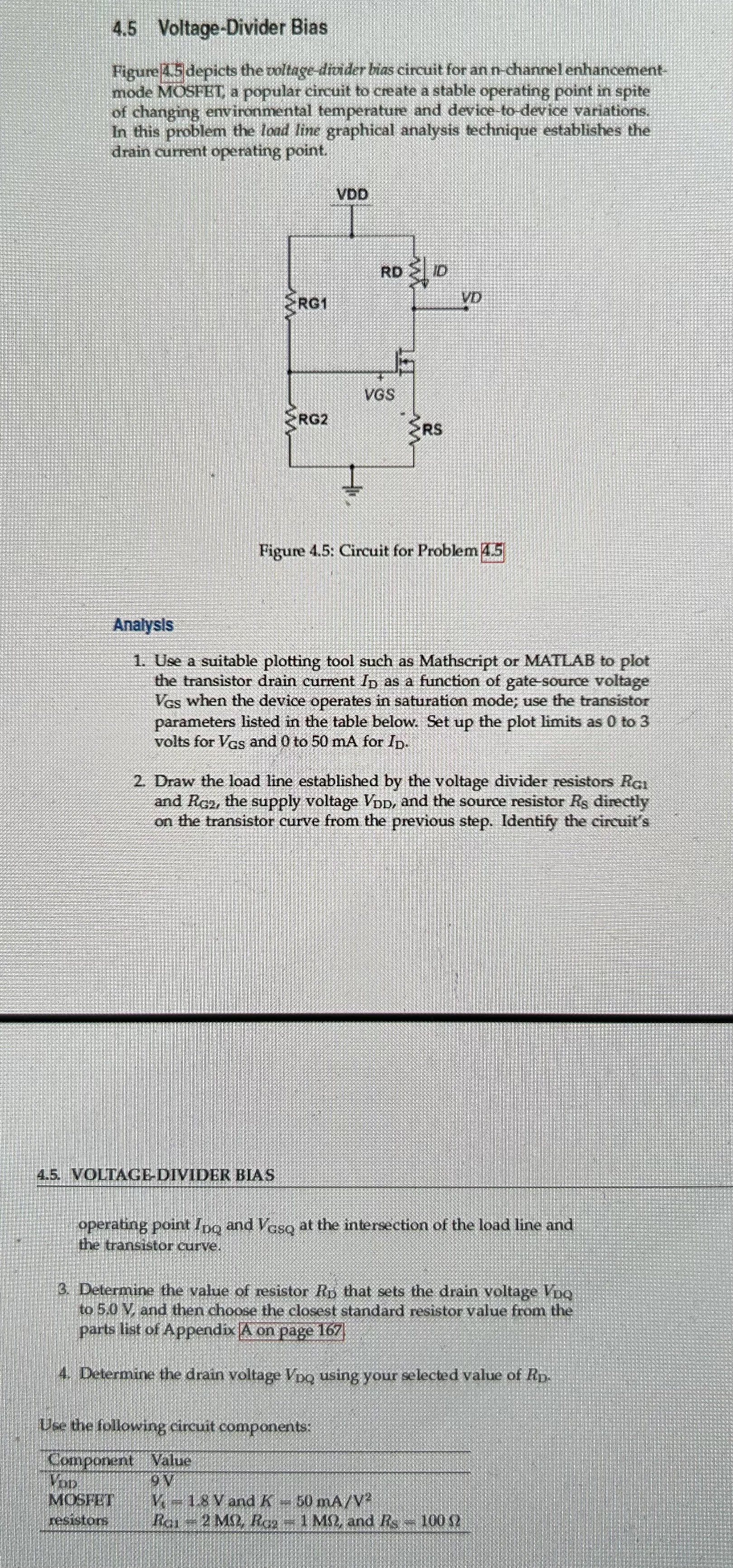
Figure depicts the voltagedivider bias circuit for an nchannel enhancementmode MOSFET, a popular circuit to create a stable operating point in spite of changing environmental temperature and devicetodevice variations. In this problem the load line graphical analysis tectinique establishes the drain current operating point.
Figure : Circuit for Problem
Analysls
Use a suitable plotting tool such as Mathscript or MATLAB to plot the transistor drain current as a function of gatesource voltage when the device operates in saturation mode; use the transistor parameters listed in the table below. Set up the plot limits as to volts for and to mA for
Draw the load line established by the voltage divider resistors and the supply voltage and the source resistor directly on the transistor curve from the previous step. Identify the circuit's
VOLTAGEDIVIDER BIAS
operating point and at the intersection of the load line and the transistor curve.
Determine the value of resistor that sets the drain voltage to V and then choose the closest standard resistor value from the parts list of Appendix A on page
Determine the drain voltage using your selected value of
Use the following circuit components:
tableComponentValuetableVoDMOSFETresistorstable V and
Step by Step Solution
There are 3 Steps involved in it
1 Expert Approved Answer
Step: 1 Unlock

Question Has Been Solved by an Expert!
Get step-by-step solutions from verified subject matter experts
Step: 2 Unlock
Step: 3 Unlock