

Question: Design a folded cascode opamp Guidelines: 1. Your circuit should be implemented by transistors using the provided transistor models 2. For each opamp, you can
 Design a folded cascode opamp
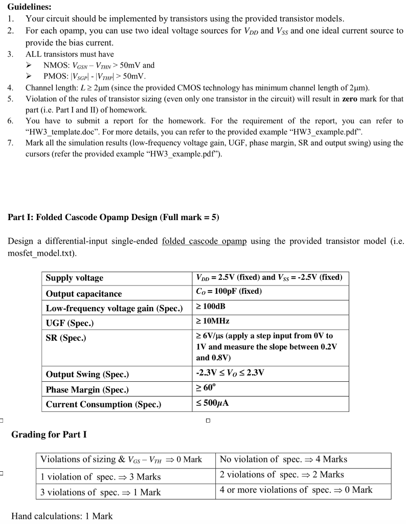
Guidelines: 1. Your circuit should be implemented by transistors using the provided transistor models 2. For each opamp, you can use two ideal voltage sources for Voo and Vss and one ideal current source to provide the bias current ALL transistors must have 3. NMOS: VGsv- VTHN> 50mV and Channel length: L 2?m (since the provided CMOS technology has minimum channel length of 2?m) part (i.e. Part I and II) of homework. "HW3_template.doc". For more details, you can refer to the provided example "HW3_example.pdf". cursors (refer the provided example "HW3_example.pdf") 4. 5. Violation of the rules of transistor sizing (even only one transistor in the circuit) will result in zero mark for that 6. You have to submit a report for the homework. For the requirement of the report, you can refer to 7. Mark all the simulation results (low-frequency voltage gain, UGF, phase margin, SR and output swing) using the Part I: Folded Cascode Opamp Design (Full mark-5) Design a differential-input single-ended folded cascode opamp using the provided transistor model (i.e mosfet model.txt) VD 2.5V (fixed) and Vss-2.5V (fixed) Co 100pF (fixed) 2 100dB 2 10MHz Supply voltage Output capacitance Low-frequency voltage gain (Spec.) UGF (Spec.) SR (Spe.) 26Vjus (apply a step input from 0V to 1V and measure the slope between 0.2V and 0.8V) Output Swing (Spec.) Phase Margin (Spec.) 60 Current Consumption (Spec.) s 500uA Grading for Part I Violations of sizing & VGs VTH0 Mark No violation of spec. > 4 Marks 1 violation of spec. > 3 Marks 3 violations of spec. 1 Mark 2 violations of spec.2 Marks 4 or more violations of spec. 0 Mark Hand calculations: 1 Mark Guidelines: 1. Your circuit should be implemented by transistors using the provided transistor models 2. For each opamp, you can use two ideal voltage sources for Voo and Vss and one ideal current source to provide the bias current ALL transistors must have 3. NMOS: VGsv- VTHN> 50mV and Channel length: L 2?m (since the provided CMOS technology has minimum channel length of 2?m) part (i.e. Part I and II) of homework. "HW3_template.doc". For more details, you can refer to the provided example "HW3_example.pdf". cursors (refer the provided example "HW3_example.pdf") 4. 5. Violation of the rules of transistor sizing (even only one transistor in the circuit) will result in zero mark for that 6. You have to submit a report for the homework. For the requirement of the report, you can refer to 7. Mark all the simulation results (low-frequency voltage gain, UGF, phase margin, SR and output swing) using the Part I: Folded Cascode Opamp Design (Full mark-5) Design a differential-input single-ended folded cascode opamp using the provided transistor model (i.e mosfet model.txt) VD 2.5V (fixed) and Vss-2.5V (fixed) Co 100pF (fixed) 2 100dB 2 10MHz Supply voltage Output capacitance Low-frequency voltage gain (Spec.) UGF (Spec.) SR (Spe.) 26Vjus (apply a step input from 0V to 1V and measure the slope between 0.2V and 0.8V) Output Swing (Spec.) Phase Margin (Spec.) 60 Current Consumption (Spec.) s 500uA Grading for Part I Violations of sizing & VGs VTH0 Mark No violation of spec. > 4 Marks 1 violation of spec. > 3 Marks 3 violations of spec. 1 Mark 2 violations of spec.2 Marks 4 or more violations of spec. 0 Mark Hand calculations: 1 Mark
Step by Step Solution
There are 3 Steps involved in it

Get step-by-step solutions from verified subject matter experts