

Question: Can you help me fill this table? My previous code from exp6: library IEEE; use IEEE.STD_LOGIC_1164.ALL; use IEEE.STD_LOGIC_ARITH.ALL; use IEEE.STD_LOGIC_UNSIGNED.ALL; entity exp6 is port (
Can you help me fill this table? My previous code from exp6:
library IEEE; use IEEE.STD_LOGIC_1164.ALL; use IEEE.STD_LOGIC_ARITH.ALL; use IEEE.STD_LOGIC_UNSIGNED.ALL;
entity exp6 is port ( clk : in std_logic; run : in std_logic; segment7: out STD_LOGIC_VECTOR(6 downto 0));
end exp6;
architecture Behavioral of exp6 is
SIGNAL y_present, y_next : STD_LOGIC_VECTOR(4 downto 0); CONSTANT S0 : STD_LOGIC_VECTOR(4 downto 0) := "00001"; CONSTANT S1 : STD_LOGIC_VECTOR(4 downto 0) := "00010"; CONSTANT S2 : STD_LOGIC_VECTOR(4 downto 0) := "00100"; CONSTANT S3 : STD_LOGIC_VECTOR(4 downto 0) := "01000"; CONSTANT S4 : STD_LOGIC_VECTOR(4 downto 0) := "10000";
begin process (run, y_present) begin case y_present is when S0 => segment7 segment7 segment7 segment7 segment7 y_next
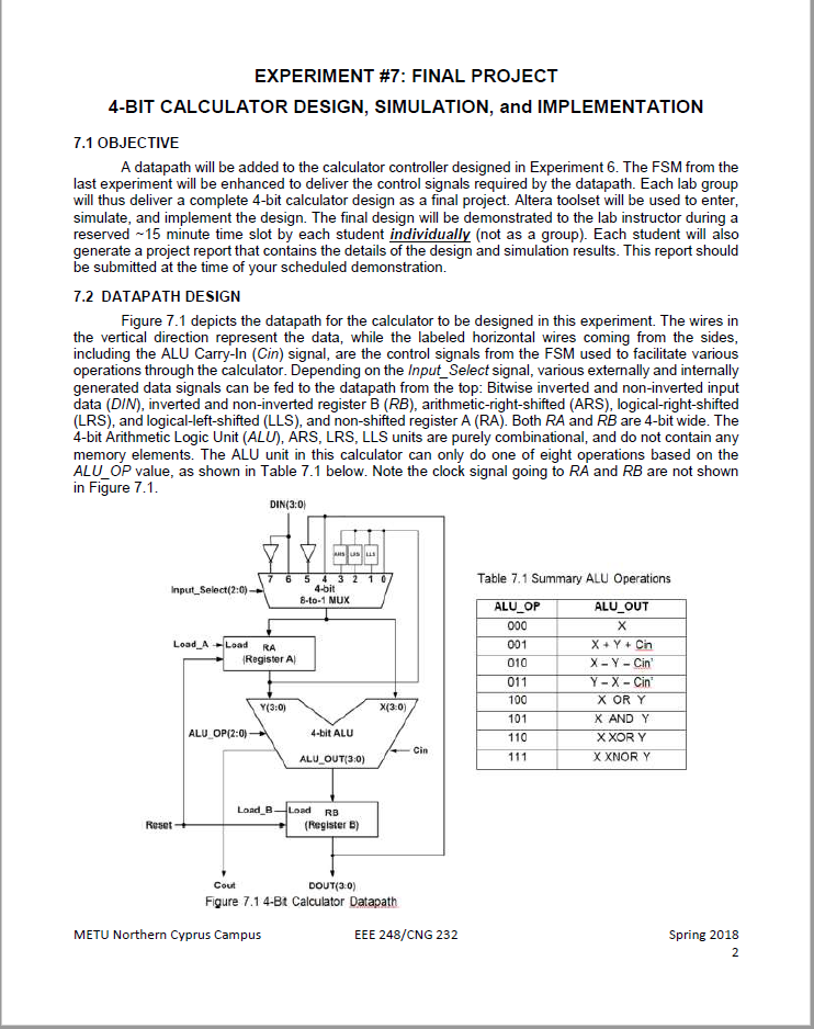
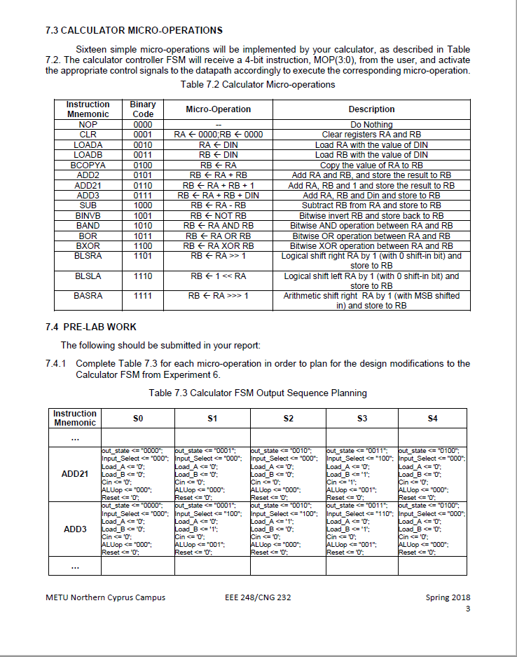
process (clk) begin if (clk'EVENT AND clk='1') then y_present EXPERIMENT #7: FINAL PROJECT 4-BIT CALCULATOR DESIGN, SIMULATION, and IMPLEMENTATION 7.1 OBJECTIVE A datapath will be added to the calculator controller designed in Experiment 6. The FSM from the last experiment will be enhanced to deliver the control signals required by the datapath. Each lab group will thus deliver a complete 4-bit calculator design as a final project. Altera toolset will be used to enter simulate, and implement the design. The final design will be demonstrated to the lab instructor during a reserved 15 minute time slot by each student individually (not as a group). Each student will also generate a project report that contains the details of the design and simulation results. This report should be submitted at the tim e of your scheduled demonstration. 7.2 DATAPATH DESIGN Figure 7.1 depicts the datapath for the calculator to be designed in this experiment. The wires in the vertical direction represent the data, while the labeled horizontal wires coming from the sides including the ALU Carry-In (Cin) signal, are the control signals from the FSM used to facilitate various operations through the calculator. Depending on the Input Select signal, various externally and internally generated data signals can be fed to the datapath from the top: Bitwise inverted and non-inverted input data (DIN), inverted and non-inverted register B (RB), arithmetic-right-shifted (ARS), logical-right-shifted (LRS), and logical-left-shifted (LLS), and non-shifted register A (RA). Both RA and RB are 4-bit wide. The 4-bit Arithmetic Logic Unit (ALU), ARS, LRS, LLS units are purely combinational, and do not contain any memory elements. The ALU unit in this calculator can only do one of eight operations based on the ALU OP value, as shown in Table 7.1 below. Note the clock signal going to RA and RB are not shown in Figure 7.1 DIN(3:0 Table 7.1 Summary ALU Operations input Select(2:0) 8-to-1 MUX ALU OP ALU OUT Load A Load RA 001 010 Register A 100 101 110 X OR Y X AND Y XXOR Y X(3.0) ALU OP12:0 4-bit ALU Cin ALU OUT(3:0) Load BLoad RB Reset (Register B) Cout DOUT(3.0) Figure 7.1 4-Bt Calculator Datapath METU Northern Cyprus Campus EEE 248/CNG 232 Spring 2018 EXPERIMENT #7: FINAL PROJECT 4-BIT CALCULATOR DESIGN, SIMULATION, and IMPLEMENTATION 7.1 OBJECTIVE A datapath will be added to the calculator controller designed in Experiment 6. The FSM from the last experiment will be enhanced to deliver the control signals required by the datapath. Each lab group will thus deliver a complete 4-bit calculator design as a final project. Altera toolset will be used to enter simulate, and implement the design. The final design will be demonstrated to the lab instructor during a reserved 15 minute time slot by each student individually (not as a group). Each student will also generate a project report that contains the details of the design and simulation results. This report should be submitted at the tim e of your scheduled demonstration. 7.2 DATAPATH DESIGN Figure 7.1 depicts the datapath for the calculator to be designed in this experiment. The wires in the vertical direction represent the data, while the labeled horizontal wires coming from the sides including the ALU Carry-In (Cin) signal, are the control signals from the FSM used to facilitate various operations through the calculator. Depending on the Input Select signal, various externally and internally generated data signals can be fed to the datapath from the top: Bitwise inverted and non-inverted input data (DIN), inverted and non-inverted register B (RB), arithmetic-right-shifted (ARS), logical-right-shifted (LRS), and logical-left-shifted (LLS), and non-shifted register A (RA). Both RA and RB are 4-bit wide. The 4-bit Arithmetic Logic Unit (ALU), ARS, LRS, LLS units are purely combinational, and do not contain any memory elements. The ALU unit in this calculator can only do one of eight operations based on the ALU OP value, as shown in Table 7.1 below. Note the clock signal going to RA and RB are not shown in Figure 7.1 DIN(3:0 Table 7.1 Summary ALU Operations input Select(2:0) 8-to-1 MUX ALU OP ALU OUT Load A Load RA 001 010 Register A 100 101 110 X OR Y X AND Y XXOR Y X(3.0) ALU OP12:0 4-bit ALU Cin ALU OUT(3:0) Load BLoad RB Reset (Register B) Cout DOUT(3.0) Figure 7.1 4-Bt Calculator Datapath METU Northern Cyprus Campus EEE 248/CNG 232 Spring 2018
Step by Step Solution
There are 3 Steps involved in it

Get step-by-step solutions from verified subject matter experts