

Question: 8. Consider the following 8-bit bidirectional synchronous shift register with parallel load capability. The notation used to represent the input/output pins is explained as follows:
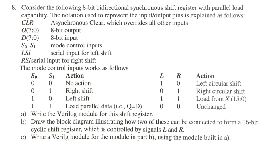
8. Consider the following 8-bit bidirectional synchronous shift register with parallel load capability. The notation used to represent the input/output pins is explained as follows: CLR Q(7:0) 8-bit output D(7:0) 8-bit input So, Si LSI RSIserial input for right shift The mode control inputs works as follows Asynchronous Clear, which overrides all other inputs mode control inputs serial input for left shift So Si Action 0 0 No action 0 L R Action Left circular shift Right circular shift 1Right shift 0Left shift 1 Load from X (15:0) 1 Load parallel data (ie, Q=D) Unchanged a) Write the Verilog module for this shift register. b) Draw the block diagram illustrating how two of these can be connected to form a 16-bit cyclic shift register, which is controlled by signals L and R. c) Write a Verilg module for the module in part b), using the module built in a) 8. Consider the following 8-bit bidirectional synchronous shift register with parallel load capability. The notation used to represent the input/output pins is explained as follows: CLR Q(7:0) 8-bit output D(7:0) 8-bit input So, Si LSI RSIserial input for right shift The mode control inputs works as follows Asynchronous Clear, which overrides all other inputs mode control inputs serial input for left shift So Si Action 0 0 No action 0 L R Action Left circular shift Right circular shift 1Right shift 0Left shift 1 Load from X (15:0) 1 Load parallel data (ie, Q=D) Unchanged a) Write the Verilog module for this shift register. b) Draw the block diagram illustrating how two of these can be connected to form a 16-bit cyclic shift register, which is controlled by signals L and R. c) Write a Verilg module for the module in part b), using the module built in a)
Step by Step Solution
There are 3 Steps involved in it

Get step-by-step solutions from verified subject matter experts