

Question: Consider the following 8-bit bidirectional synchronous shift register with parallel load capability. The notation used to represent the input/output pins is explained as follows: CLR
CLR Asynchronous Clear, which overrides all other inputs
Q(7:0) 8-bit output
D(7:0) 8-bit input
S0, S1mode control inputs
LSI serial input for left shift
RSI serial input for right shift
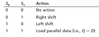
The mode control inputs work as follows:
(a) Write a Verilog module for this shift register.
(b) Draw a block diagram illustrating how two of these can be connected to form a 16-bit cyclic shift register, which is controlled by signals L and R. If L = 1 and R = 0, the 16-bit register is cycled left. If L = 0 and R = 1, the register is cycled right. If L = R = 1, the 16-bit register is loaded from X(15:0). If L = R = 0, the register is unchanged.
(c) Write a Verilog module for the module in part (b), using the module built in (a).
s, So Action No action Right shift Left shift Load parallel data (i.e., Q = D) 1 1
Step by Step Solution
3.46 Rating (159 Votes )
There are 3 Steps involved in it
a module shift8Q D CLR CLK S0 ... View full answer

Get step-by-step solutions from verified subject matter experts