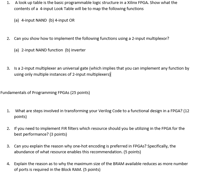
Question: A look up table is the basic programmable logic structure in a Xilinx FPGA. Show what the contents of a 4-input Look Table will be

A look up table is the basic programmable logic structure in a Xilinx FPGA. Show what the contents of a 4-input Look Table will be to map the following functions 4-input NAND (b) 4-input OR Can you show how to implement the following functions using a 2-input multiplexor? 2-input NAND function (b) inverter Is a 2-input multiplexer an universal gate (which implies that you can implement any function by using only multiple instances of 2-input multiplexers) Fundamentals of Programming FPGAs What are steps involved in transforming your Verilog Code to a functional design in a FPGA? If you need to implement FIR filters which resource should you be utilizing in the FPGA for the best performance? Can you explain the reason why one-hot encoding is preferred in FPGAs? Specifically, the abundance of what resource enables this recommendation. Explain the reason as to why the maximum size of the BRAM available reduces as more number of ports is required in the Block RAM
Step by Step Solution
There are 3 Steps involved in it

Get step-by-step solutions from verified subject matter experts


