

Question: A static random access memory (SRAM) unit cell for storing one bit of information can be constructed using several CMOS transistors as shown below:
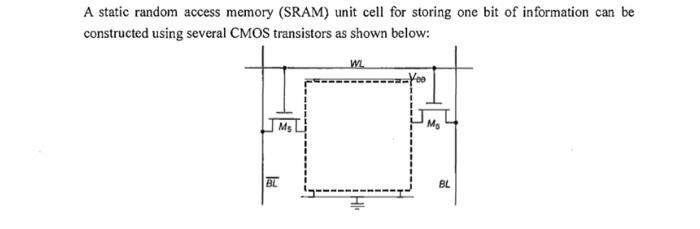
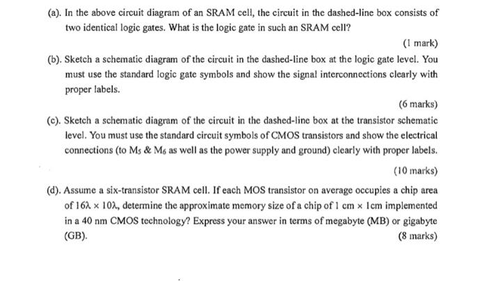
A static random access memory (SRAM) unit cell for storing one bit of information can be constructed using several CMOS transistors as shown below: Yoo Mo BL BL (a). In the above circuit diagram of an SRAM cell, the circuit in the dashed-line box consists of two identical logic gates. What is the logic gate in such an SRAM cell? (1 mark) (b). Sketch a schematic diagram of the circuit in the dashed-line box at the logic gate level. You must use the standard logic gate symbols and show the signal interconnections clearly with proper labels. (6 marks) (c). Sketch a schematic diagram of the circuit in the dashed-line box at the transistor schematic level. You must use the standard circuit symbols of CMOS transistors and show the electrical connections (to Ms & M6 as well as the power supply and ground) clearly with proper labels. (10 marks) (d). Assume a six-transistor SRAM cell. If each MOS transistor on average occupies a chip area of 162 x 102, determine the approximate memory size of a chip of 1 cm x 1cm implemented in a 40 nm CMOS technology? Express your answer in terms of megabyte (MB) or gigabyte (GB). (8 marks)
Step by Step Solution
There are 3 Steps involved in it
a The logic gate in the SRAM cell circuit is a crosscoupled inverter or a NOR gate b Here is a schem... View full answer

Get step-by-step solutions from verified subject matter experts