

Question: b ) Draw the circuit diagram of a basic logic element ( BLE ) used in an FPGA and show how its functionality can be
b Draw the circuit diagram of a basic logic element BLE used in an FPGA and show how its functionality can be programmed and reprogrammed in the field. Describe the three different methods which can be used for storing the programming bits and compare and contrast them citing advantages and disadvantages of each.
c Draw the diagram of an FPLS with storage elements, primary inputs and three primary outputs and explain how multiplexers can be used to implementing the programming of the OR plane, the AND plane and the final output stage of exclusive OR gates.
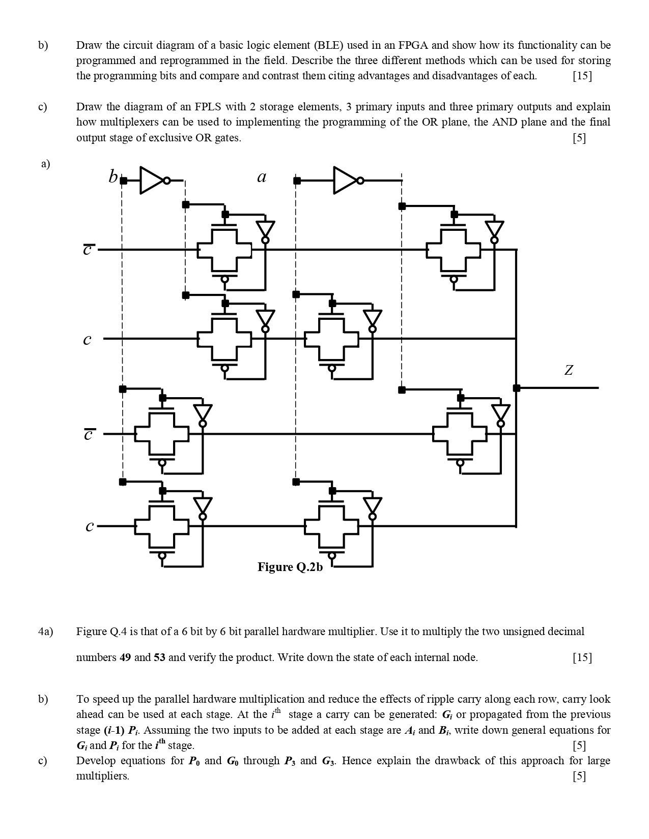
a
a Figure Q is that of a bit by bit parallel hardware multiplier. Use it to multiply the two unsigned decimal numbers and and verify the product. Write down the state of each internal node.
b To speed up the parallel hardware multiplication and reduce the effects of ripple carry along each row, carry look ahead can be used at each stage. At the itext th stage a carry can be generated: boldsymbolGboldsymboli or propagated from the previous stage iboldsymbolPboldsymboli Assuming the two inputs to be added at each stage are boldsymbolAboldsymboli and boldsymbolBboldsymboli write down general equations for boldsymbolGboldsymboli and boldsymbolPboldsymboli for the boldsymbolitext th stage.
c Develop equations for boldsymbolPmathbf and boldsymbolGmathbf through boldsymbolPmathbf and boldsymbolGmathbf Hence explain the drawback of this approach for large multipliers.
Step by Step Solution
There are 3 Steps involved in it
1 Expert Approved Answer
Step: 1 Unlock

Question Has Been Solved by an Expert!
Get step-by-step solutions from verified subject matter experts
Step: 2 Unlock
Step: 3 Unlock