

Question: Bus Memory Bus Address Memory unit 4096 X 16 Address Write Read AR LD INR CLR TAR PC I LD INR CLR Write Read AR
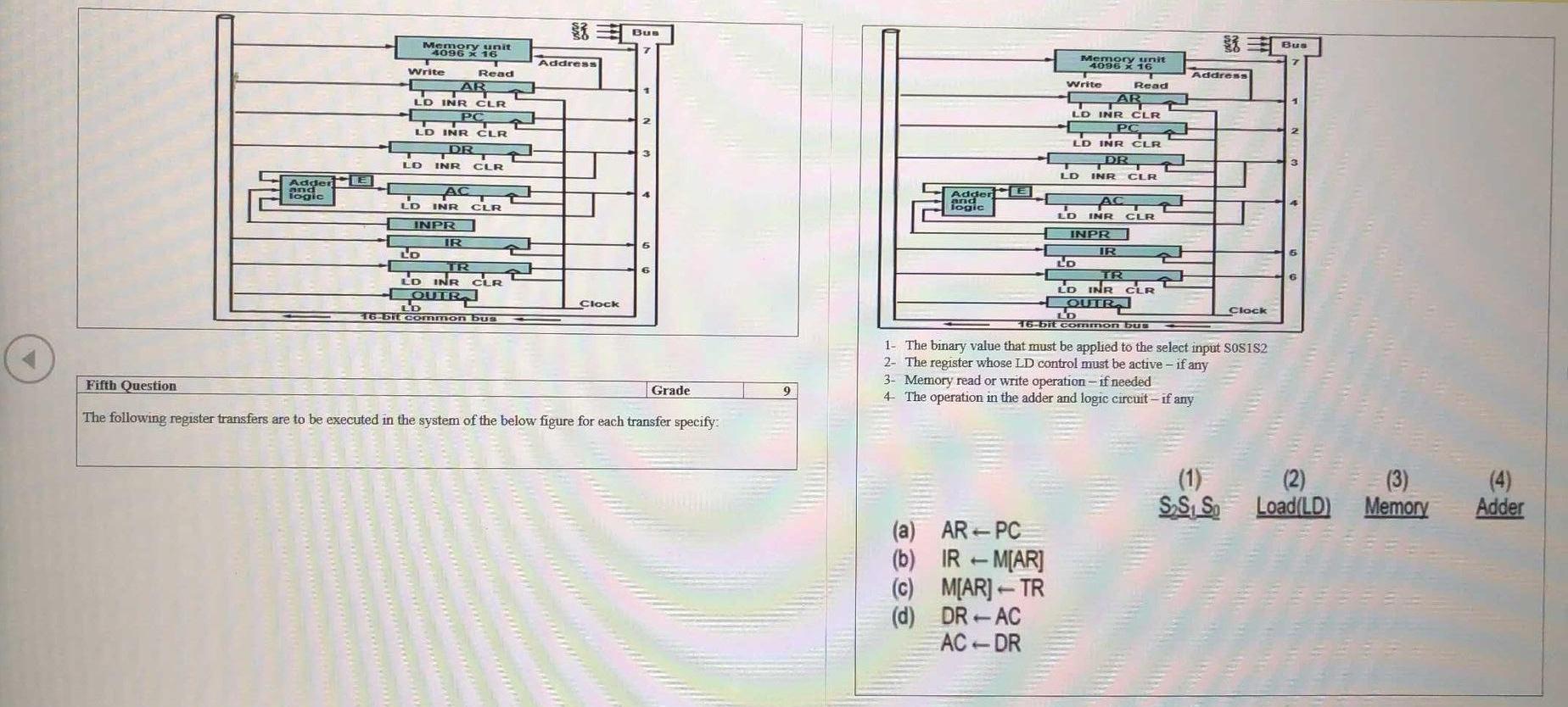
Bus Memory Bus Address Memory unit 4096 X 16 Address Write Read AR LD INR CLR TAR PC I LD INR CLR Write Read AR LD INR CLR PC LD INR CLR DR LD INR CLR DR Adder logic E Adder and logic LD INR CLR IE AC LD INR CLR INPR IR Lo TR LD INR CLR OIR LD 16 bit common bus AC LD INR CLR INPR IR LD IR LO NR CLR 6 Clock Clock 16-bit common bus 1- The binary value that must be applied to the select input SOS1S2 2- The register whose LD control must be active - if any 3- Memory read or write operation - if needed 4 The operation in the adder and logic circuit - if any Fifth Question Grade The following register transfers are to be executed in the system of the below figure for each transfer specify: SS, SO (2) Load(LD) (3) Memory Adder (a) AR - PC (b) IR M[AR] () M[AR]- TR (d) DRAC AC - DR
Step by Step Solution
There are 3 Steps involved in it

Get step-by-step solutions from verified subject matter experts