

Question: c. Arithmetic logical unit (ALU). In this part you will complete the design of an ALU that computes the arithmetic and logical operations specified in
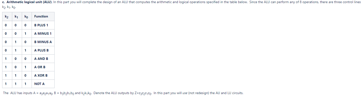

c. Arithmetic logical unit (ALU). In this part you will complete the design of an ALU that computes the arithmetic and logical operations specified in the table below. Since the ALU can perform any of 8 operations, there are three control lines k2, k1, ko Function k2 kg ko 0 0 0 0 B PLUS 1 0 A MINUS 1 B MINUS A o 1 1 A PLUS B 1 oo A AND B 1 1 A OR B 1 1 0 A XOR B 1 1 1 NOT A The ALU has inputs A = azaza1a0. B = b3b2b1bo and kzk ko. Denote the ALU outputs by Z=23222120. In this part you will use (not redesign) the AU and LU circuits. 1. List all AU inputs and outputs. List all LU inputs and outputs. 2. Draw a "box" to represent the AU and another "box" to represent the LU. Each box must have all inputs and outputs labeled, and the box itself must be labeled. Complete the ALU circuit by interconnecting the AU and LU (be sure to label all wires). Use MUXes as needed and as few additional gates as possible. Note: You may wish to use a dual (or 3-ary or quad) MUX, which is a chip that has 2 or 3 or 4) MUXes - all of which share the same select inputs. E.g. a dual 4:1 MUX or a quad 2:1 MUX. Notation: Use "slash N" notation to denote that a wire is a bundle of N wires (see e.g. the figure on p. 51 of Lumetta's notes). c. Arithmetic logical unit (ALU). In this part you will complete the design of an ALU that computes the arithmetic and logical operations specified in the table below. Since the ALU can perform any of 8 operations, there are three control lines k2, k1, ko Function k2 kg ko 0 0 0 0 B PLUS 1 0 A MINUS 1 B MINUS A o 1 1 A PLUS B 1 oo A AND B 1 1 A OR B 1 1 0 A XOR B 1 1 1 NOT A The ALU has inputs A = azaza1a0. B = b3b2b1bo and kzk ko. Denote the ALU outputs by Z=23222120. In this part you will use (not redesign) the AU and LU circuits. 1. List all AU inputs and outputs. List all LU inputs and outputs. 2. Draw a "box" to represent the AU and another "box" to represent the LU. Each box must have all inputs and outputs labeled, and the box itself must be labeled. Complete the ALU circuit by interconnecting the AU and LU (be sure to label all wires). Use MUXes as needed and as few additional gates as possible. Note: You may wish to use a dual (or 3-ary or quad) MUX, which is a chip that has 2 or 3 or 4) MUXes - all of which share the same select inputs. E.g. a dual 4:1 MUX or a quad 2:1 MUX. Notation: Use "slash N" notation to denote that a wire is a bundle of N wires (see e.g. the figure on p. 51 of Lumetta's notes)
Step by Step Solution
There are 3 Steps involved in it

Get step-by-step solutions from verified subject matter experts