

Question: circuit diagram, clearly label the source (S), gate (G), and drain (D) of the MOSFET. Is the transistor an NMOS or a PMOS device?
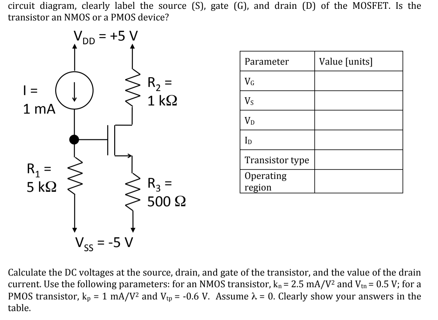
circuit diagram, clearly label the source (S), gate (G), and drain (D) of the MOSFET. Is the transistor an NMOS or a PMOS device? VDD = +5 V |= 1 mA R = 5 RS Vss = -5 V R = 1 R3 = 500 Parameter VG Vs VD ID Transistor type Operating region Value [units] Calculate the DC voltages at the source, drain, and gate of the transistor, and the value of the drain current. Use the following parameters: for an NMOS transistor, kn = 2.5 mA/V and Vtn = 0.5 V; for a PMOS transistor, kp = 1 mA/V and Vtp = -0.6 V. Assume = 0. Clearly show your answers in the table.
Step by Step Solution
★★★★★
3.36 Rating (168 Votes )
There are 3 Steps involved in it
1 Expert Approved Answer
Step: 1 Unlock

Question Has Been Solved by an Expert!
Get step-by-step solutions from verified subject matter experts
Step: 2 Unlock
Step: 3 Unlock