

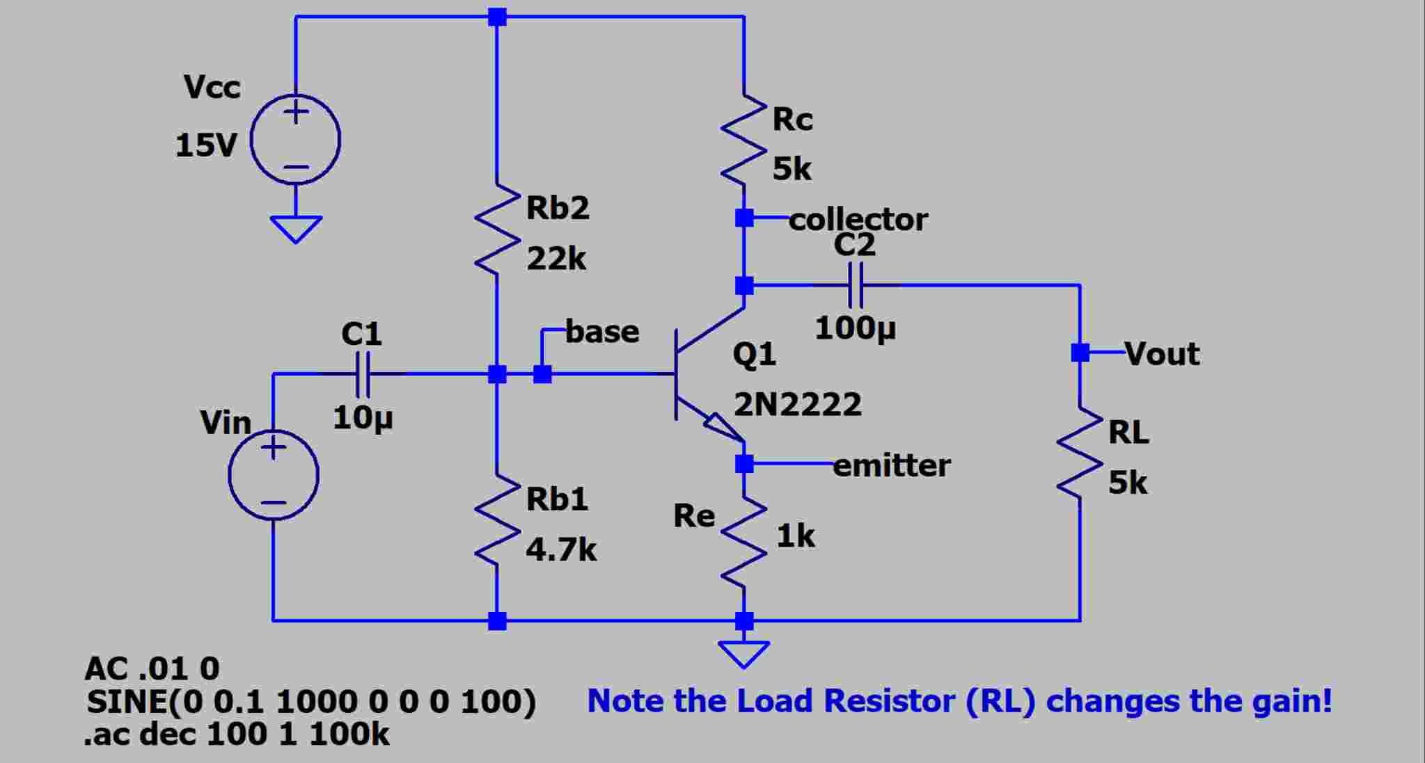
Question: Common Emitter Amplifier using 2 N 2 2 2 2 with bypass capacitors and dc blocking capacitors with a designed gain of - 5 ,
Common Emitter Amplifier using N with bypass capacitors and dc blocking
capacitors with a designed gain of circuit diagram with operating point information on
a single page, transfer function frequency response plot in dB on a second single page
and a one page explanation. All bypass capacitors and dc blocking capacitors are uF
aC qec IUU IUUK ac qec UU UUK
Step by Step Solution
There are 3 Steps involved in it
1 Expert Approved Answer
Step: 1 Unlock

Question Has Been Solved by an Expert!
Get step-by-step solutions from verified subject matter experts
Step: 2 Unlock
Step: 3 Unlock