

Question: last two digit is 01 Objective: Build a Common Emitter amplifier circuit and measure the DC parameters, the AC input resistance, and the voltage gain.
 last two digit is 01
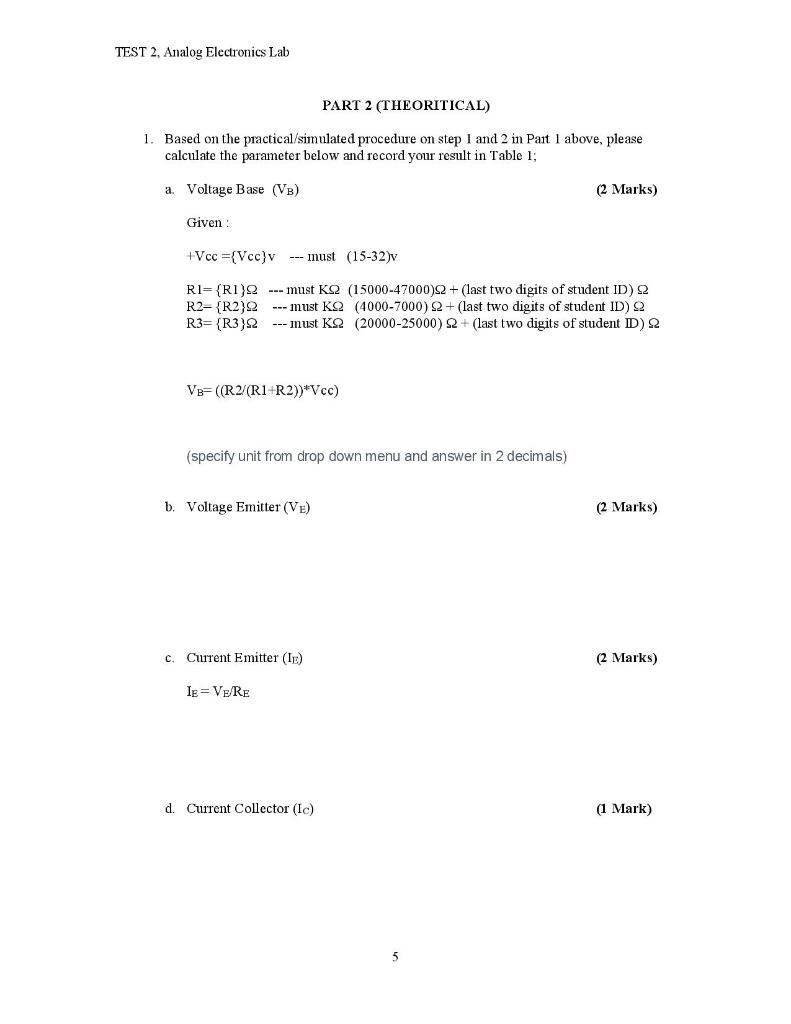
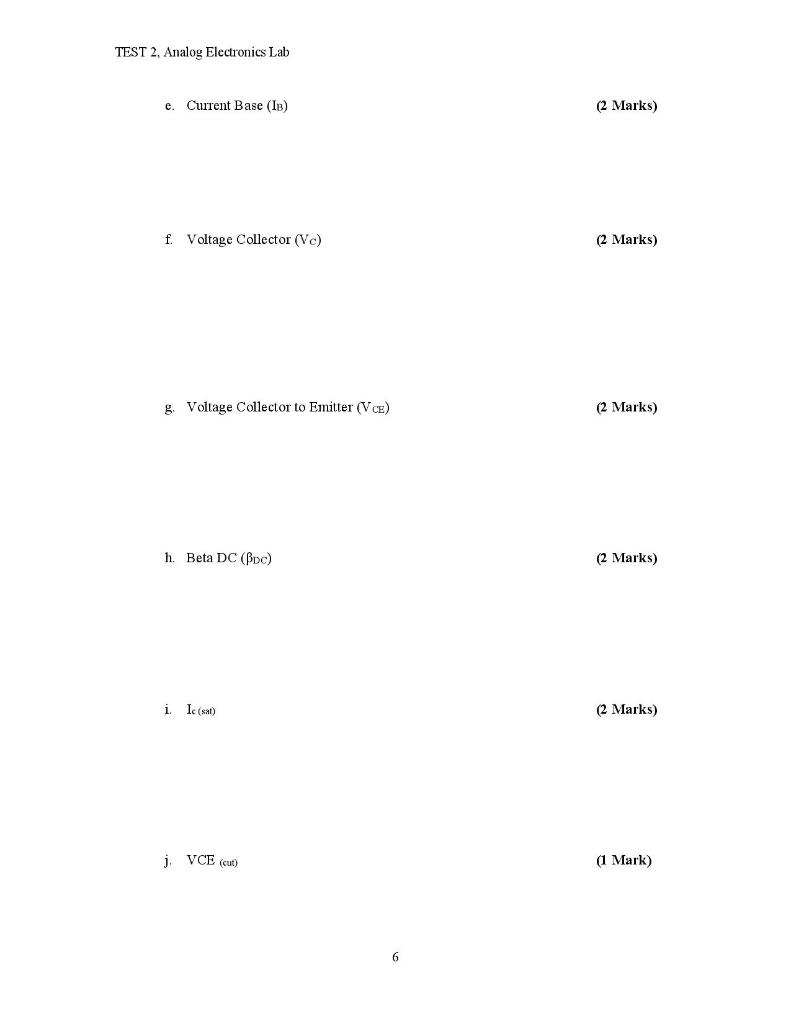
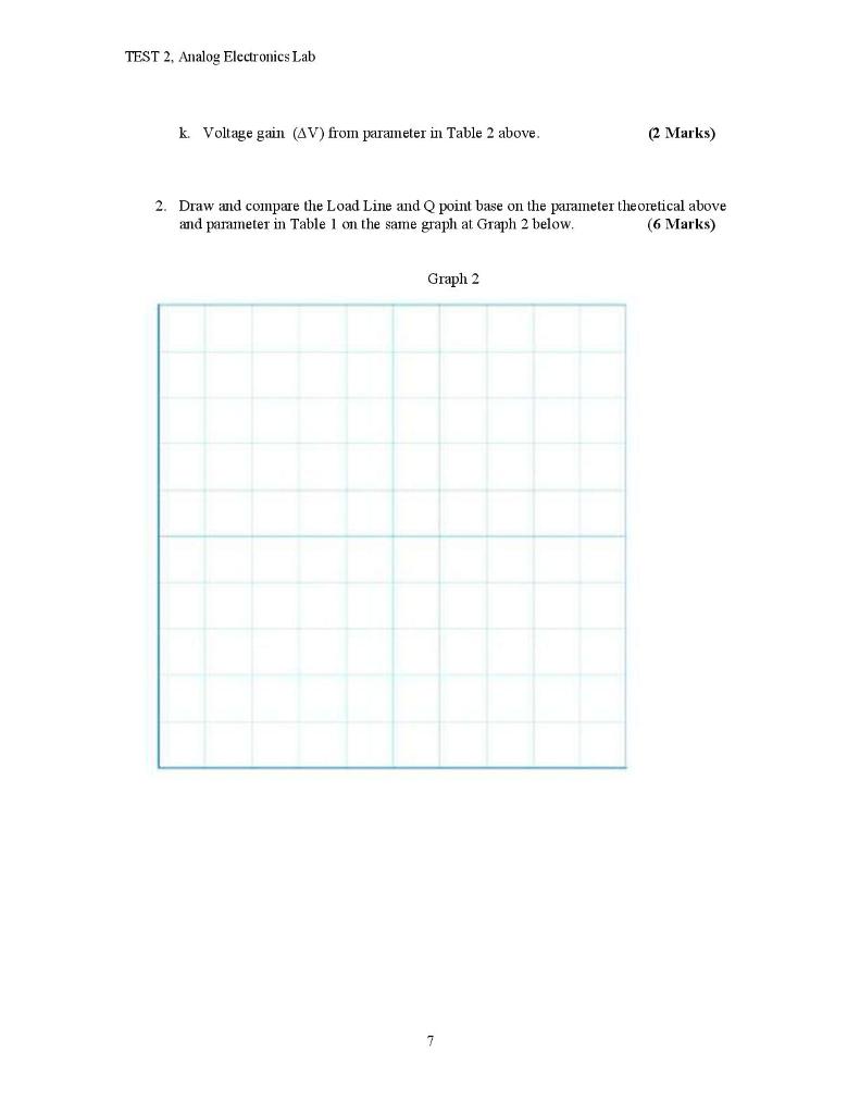
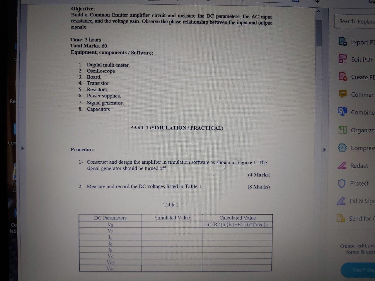
Objective: Build a Common Emitter amplifier circuit and measure the DC parameters, the AC input resistance, and the voltage gain. Observe the phase relationship between the input and output signals Search 'Replace Time: 3 hours Total Marks: 60 Equipment, components / Software: Export PC Edit PDF Create PD 1. Digital multi-meter 2. Oscilloscope. 3. Board 4. Transistor 5. Resistors 6. Power supplies 7. Signal generator 8. Capacitors Commen Re Combine PART 1 (SIMULATION / PRACTICAL) El Organize Con Procedure Compress 1- Construct and design the amplifier in simulation software as shown in Figure 1. The signal generator should be turned off. (4 Marks) Redact Protect 2- Measure and record the DC voltages listed in Table 1. (8 Marks) Fill & Sigr Table 1 Simulated Value Send for Calculated Value ={({R}(R1+R21*{Vee)) lab DC Parameters VB VE Ig le Is Create, edit and forms & agre VE VRC Free 7-Da TEST 2. Analog Electronics Lab PART 2 (THEORITICAL) 1. Based on the practical/simulated procedure on step 1 and 2 in Part 1 above, please calculate the parameter below and record your result in Table 1; a. Voltage Base (VB) (2 Marks) Given : +Vcc={Vcc}v --- must (15-32) RI={RI) --- must K12 (15000-47000)2 + (last two digits of student ID) 2 R2-{R2} --- must KO (4000-7000) 2+ (last two digits of student ID) R3= {R322 --- must KQ (20000-25000) 2+ (last two digits of student D) VB=((R2/(R1+R2))*Vcc) (specify unit from drop down menu and answer in 2 decimals) b. Voltage Emitter (VE) (2 Marks) c. Current Emitter (IE) (2 Marks) le = VERE d. Current Collector (Ic) (1 Mark) 5 TEST 2. Analog Electronics Lab e Current Base (15) (2 Marks) f. Voltage Collector (Vc) (2 Marks) g. Voltage Collector to Emitter (VCE) (2 Marks) h. Beta DC (BC) (2 Marks) i. Ic (sat) (2 Marks) j VCE (cut) (1 Mark) 6 TEST 2, Analog Electronics Lab k Voltage gain (AV) from parameter in Table 2 above. (2 Marks) 2. Draw and compare the Load Line and Q point base on the parameter theoretical above and parameter in Table 1 on the same graph at Graph 2 below. (6 Marks) Graph 2 7 Objective: Build a Common Emitter amplifier circuit and measure the DC parameters, the AC input resistance, and the voltage gain. Observe the phase relationship between the input and output signals Search 'Replace Time: 3 hours Total Marks: 60 Equipment, components / Software: Export PC Edit PDF Create PD 1. Digital multi-meter 2. Oscilloscope. 3. Board 4. Transistor 5. Resistors 6. Power supplies 7. Signal generator 8. Capacitors Commen Re Combine PART 1 (SIMULATION / PRACTICAL) El Organize Con Procedure Compress 1- Construct and design the amplifier in simulation software as shown in Figure 1. The signal generator should be turned off. (4 Marks) Redact Protect 2- Measure and record the DC voltages listed in Table 1. (8 Marks) Fill & Sigr Table 1 Simulated Value Send for Calculated Value ={({R}(R1+R21*{Vee)) lab DC Parameters VB VE Ig le Is Create, edit and forms & agre VE VRC Free 7-Da TEST 2. Analog Electronics Lab PART 2 (THEORITICAL) 1. Based on the practical/simulated procedure on step 1 and 2 in Part 1 above, please calculate the parameter below and record your result in Table 1; a. Voltage Base (VB) (2 Marks) Given : +Vcc={Vcc}v --- must (15-32) RI={RI) --- must K12 (15000-47000)2 + (last two digits of student ID) 2 R2-{R2} --- must KO (4000-7000) 2+ (last two digits of student ID) R3= {R322 --- must KQ (20000-25000) 2+ (last two digits of student D) VB=((R2/(R1+R2))*Vcc) (specify unit from drop down menu and answer in 2 decimals) b. Voltage Emitter (VE) (2 Marks) c. Current Emitter (IE) (2 Marks) le = VERE d. Current Collector (Ic) (1 Mark) 5 TEST 2. Analog Electronics Lab e Current Base (15) (2 Marks) f. Voltage Collector (Vc) (2 Marks) g. Voltage Collector to Emitter (VCE) (2 Marks) h. Beta DC (BC) (2 Marks) i. Ic (sat) (2 Marks) j VCE (cut) (1 Mark) 6 TEST 2, Analog Electronics Lab k Voltage gain (AV) from parameter in Table 2 above. (2 Marks) 2. Draw and compare the Load Line and Q point base on the parameter theoretical above and parameter in Table 1 on the same graph at Graph 2 below. (6 Marks) Graph 2 7
Step by Step Solution
There are 3 Steps involved in it

Get step-by-step solutions from verified subject matter experts